Hybrid beam deposition system and methods for fabricating metal oxide-zno films, p-type zno films, and zno-based II-VI compound semiconductor devices

a technology of metal oxide alloy and beam deposition system, which is applied in the direction of crystal growth process, semiconductor laser, polycrystalline material growth, etc., can solve the problems of limited oxidation maximum rate of high-quality zno film growth, difficult to prepare a target satisfying, and limitations of conventional cvd techniques, etc., to achieve the effect of increasing the flux density of available reactive oxygen

Inactive Publication Date: 2006-10-19
MOXTRONICS
View PDF8 Cites 49 Cited by
  • Summary
  • Abstract
  • Description
  • Claims
  • Application Information

AI Technical Summary

Benefits of technology

[0012] A hybrid beam deposition (HBD) system and methods according to the present invention utilizes a unique combination of a pulsed laser deposition (PLD) technique and equipment with equipment and techniques that provide a radical oxygen rf-plasma stream to effectively increase the flux density of available reactive oxygen at a deposition substrate for the effect...

Problems solved by technology

Unfortunately, it is very difficult to prepare a target satisfying these conditions.
Over pressurization of the oxygen constituent, however, in this MBE technique is limited due to the adverse effects of oxidation on the MBE equipment, which limits the maximum rate of high-quality ZnO film growth.
Conventional CVD techniques are also...

Method used


Image

  • Hybrid beam deposition system and methods for fabricating metal oxide-zno films, p-type zno films, and zno-based II-VI compound semiconductor devices
  • Hybrid beam deposition system and methods for fabricating metal oxide-zno films, p-type zno films, and zno-based II-VI compound semiconductor devices
  • Hybrid beam deposition system and methods for fabricating metal oxide-zno films, p-type zno films, and zno-based II-VI compound semiconductor devices

Examples


Embodiment Construction

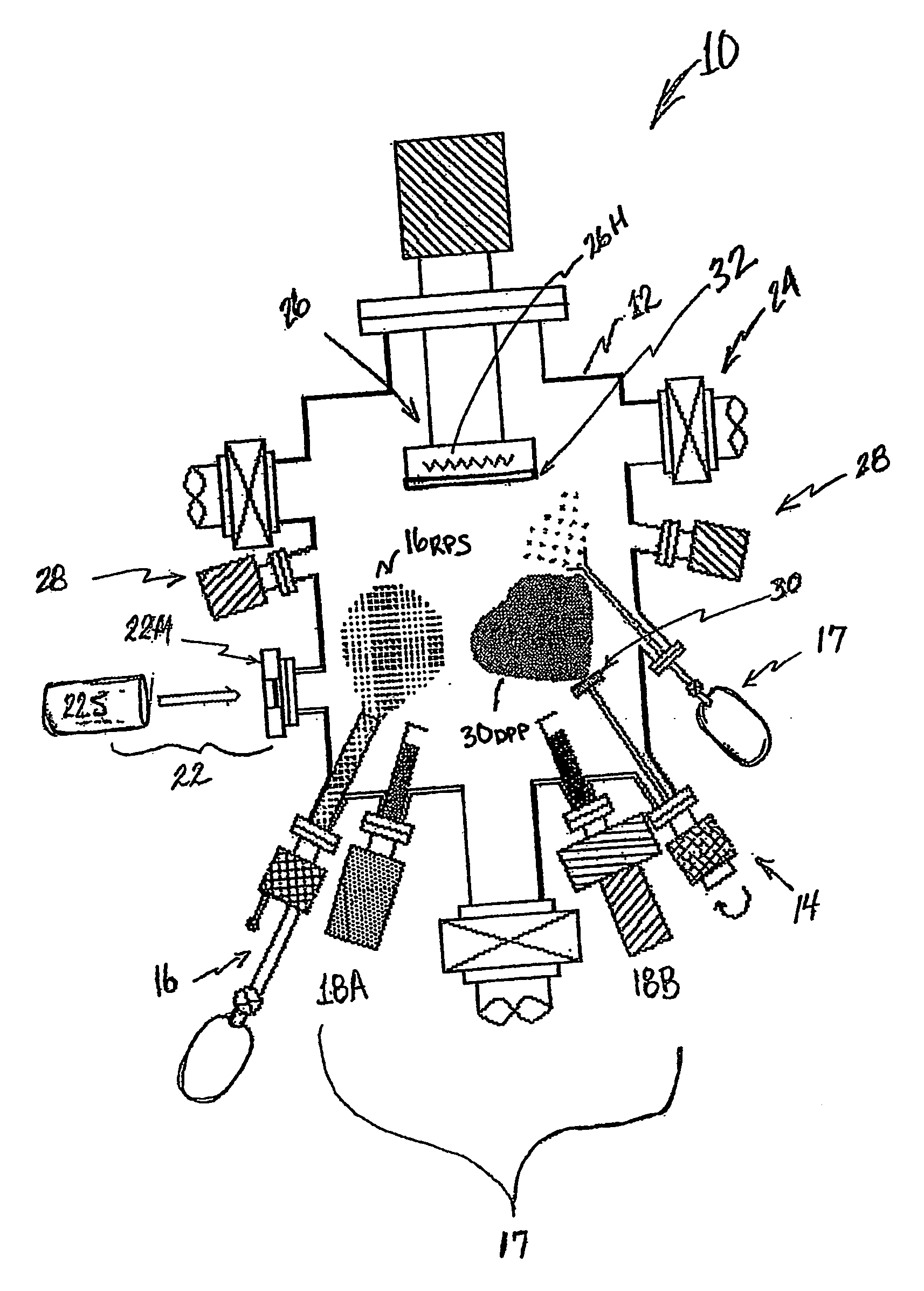
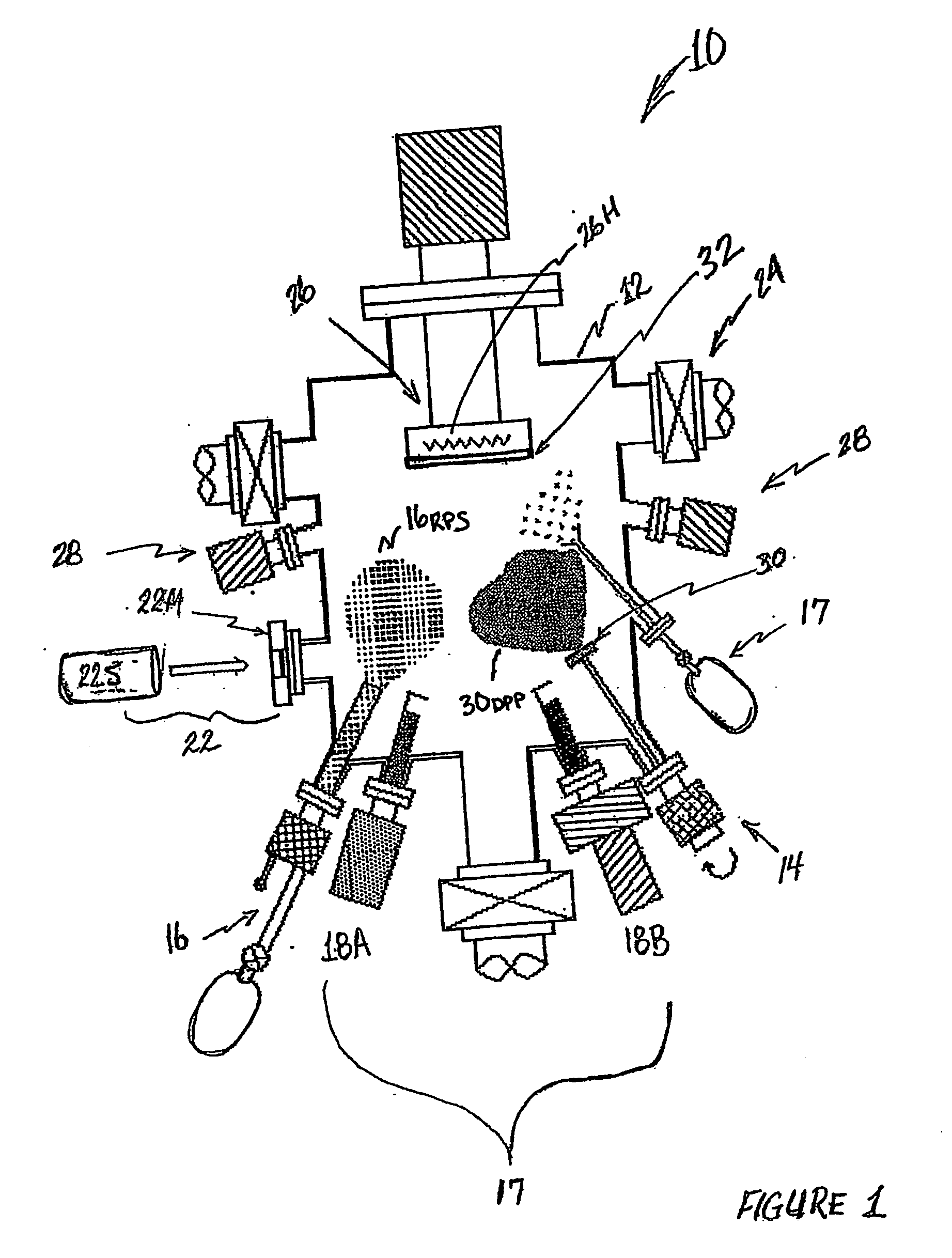
[0050] Referring now to the drawings wherein like reference numerals indicate corresponding or similar elements throughout the several views, FIG. 1 illustrates a hybrid beam deposition (HBD) system 10 of the present invention for synthesizing high quality metal oxide films such as ZnO thin film layers and fabricating semiconductor devices embodying such n-type and p-type ZnO thin film layers. The HBD system 10 utilizes a unique combination of pulsed laser deposition (PLD) with a radical oxygen rf-plasma steam to effectively increase the flux density of available reactive oxygen for the effective synthesis of metal oxide thin layer films. The HBD system 10 further integrates molecular beam epitaxy (MBE) and / or chemical vapor deposition (CVD) techniques in combination with the PLD equipment and the radical oxygen rf-plasma stream to synthesize thin films that include dopant atoms.

[0051] The HBD system 10 includes a deposition chamber 12, a target assembly 14, an rf reactive gas sour...


PUM

PropertyMeasurementUnit
Pressureaaaaaaaaaa
Pressureaaaaaaaaaa
Temperatureaaaaaaaaaa

Abstract

A hybrid beam deposition (HBD) system and methods according to the present invention utilizes a unique combination of pulsed laser deposition (PLD) technique and equipment with equipment and techniques that provide a radical oxygen rf-plasma stream to effectively increase the flux density of available reactive oxygen at a deposition substrate for the effective synthesis of metal oxide thin films. The HBD system and methods of the present invention further integrate molecular beam epitaxy (MBE) and/or chemical vapor deposition (CVD) techniques and equipment in combination with the PLD equipment and technique and the radical oxygen rf-plasma stream to provide elemental source materials for the synthesis of undoped and/or doped metal oxide thin films as well as synthesis of undoped and/or doped metal-based oxide alloy thin films.

Description

CROSS-REFERENCE TO RELATED APPLICATIONS [0001] The present application is based upon and claims priority from U.S. provisional patent application Ser. No. 60 / 406,500, filed 28 Aug. 2002, entitled HYBRID BEAM DEPOSITION SYSTEM AND METHOD FOR FABRICATING METAL OXIDE ZNO FILMS, P-TYPE ZNO FILMS, AND ZNO-BASED II-VI GROUP COMPOUND SEMICONDUCTOR DEVICES.BACKGROUND OF THE INVENTION [0002] (1) FIELD OF THE INVENTION [0003] This invention relates generally to systems and methods for forming metal oxide and metal-based oxide alloy films for semiconductor applications, and, more particularly, to a hybrid beam deposition (HBD) system and methods for fabricating metal oxide ZnO films, p-type ZnO films, and ZnO-based II-VI group compound semiconductor devices such as light-emitting diodes (LEDs), laser diodes (LDs), photodetectors, and gas sensors and bipolar / unipolar semiconductor devices such as heterojunction bipolar transistors (HBT) and field-effect transistors (FET)s. [0004] (2) DESCRIPTIO...

Claims


Application Information

Patent Timeline
IPC IPC(8): H05H1/24C23C16/00C23C14/00C30B23/08C23C14/08C23C14/28C30B23/02C30B25/02C30B25/10C30B29/16C30B35/00H01L21/205H01L21/265H01L21/363H01L21/443H01L29/205H01L29/267H01L31/04H01L33/00
CPCC23C14/0026H01L21/02661C23C14/081C23C14/22C23C14/28C23C14/547C30B23/02C30B25/02C30B25/10C30B29/16C30B35/00H01J37/32357H01L21/265H01L21/443H01L33/0083H01S2304/00H05H1/24C23C14/0031H01L21/02631H01L21/02579H01L21/02565H01L21/0256H01L21/02557H01L21/0237H01L21/0242H01L21/02472H01L21/02521H01L21/02554
Inventor WHITE, HENRY W.RYU, YUNGRYELLEE, TAE-SEOK
Owner MOXTRONICS
Why Eureka
Try Eureka