Method of surface treatment of group III nitride crystal film, group III nitride crystal substrate, group III nitride crystal substrate with epitaxial layer, and semiconductor device

a technology of nitride crystal film and surface treatment method, which is applied in the direction of after-treatment details, manufacturing tools, lapping machines, etc., can solve the problems of difficult to further reduce the surface roughness, the crystallinity decrease, and the inability to form satisfactory quality semiconductor devices on such a substrate. , to achieve the effect of efficient production and efficient formation

Inactive Publication Date: 2006-10-26
SUMITOMO ELECTRIC IND LTD
View PDF7 Cites 48 Cited by
  • Summary
  • Abstract
  • Description
  • Claims
  • Application Information

AI Technical Summary

Benefits of technology

[0010] In order to efficiently produce a Group III nitride crystal substrate that can be used for semiconductor devices, it is an object of the present invention to provide a method of surface treatment of a Group III nitride crystal film in which a satisfactory quality smooth surface with a thin affected layer can be efficiently formed on the Group III nitride crystal film.
[0019] According to the present invention, a satisfactory quality smooth surface with a thin affected layer can be efficiently formed on a Group III nitride crystal film, and thus a Group III nitride crystal substrate that can be used for semiconductor devices can be efficiently produced.

Problems solved by technology

As the thickness of the affected layer of the Group III nitride crystal substrate increases, and as the surface roughness thereof increases, the surface quality of the substrate degrades, resulting in an increase in surface irregularities of a Group III nitride crystal layer, which is formed on the surface of the Group III nitride crystal film by epitaxial growth, and a decrease in the crystallinity.
Therefore, semiconductor devices with satisfactory quality cannot be formed on such a substrate.
However, in the method of dry-etching the surface of the Group III nitride crystal substrate, although the affected layer can be removed, it is difficult to further decrease the surface roughness.
However, since the Group III nitride crystal film is hard and has low reactivity, the polishing rate is very low and such a known polishing is an inefficient method.
However, in the polishing method disclosed in Japanese Unexamined Patent Application Publication No. 2004-311575, it is difficult to further improve the surface smoothness because the slurry contains hard abrasive grains.

Method used


Image

  • Method of surface treatment of group III nitride crystal film, group III nitride crystal substrate, group III nitride crystal substrate with epitaxial layer, and semiconductor device
  • Method of surface treatment of group III nitride crystal film, group III nitride crystal substrate, group III nitride crystal substrate with epitaxial layer, and semiconductor device
  • Method of surface treatment of group III nitride crystal film, group III nitride crystal substrate, group III nitride crystal substrate with epitaxial layer, and semiconductor device

Examples


example 1

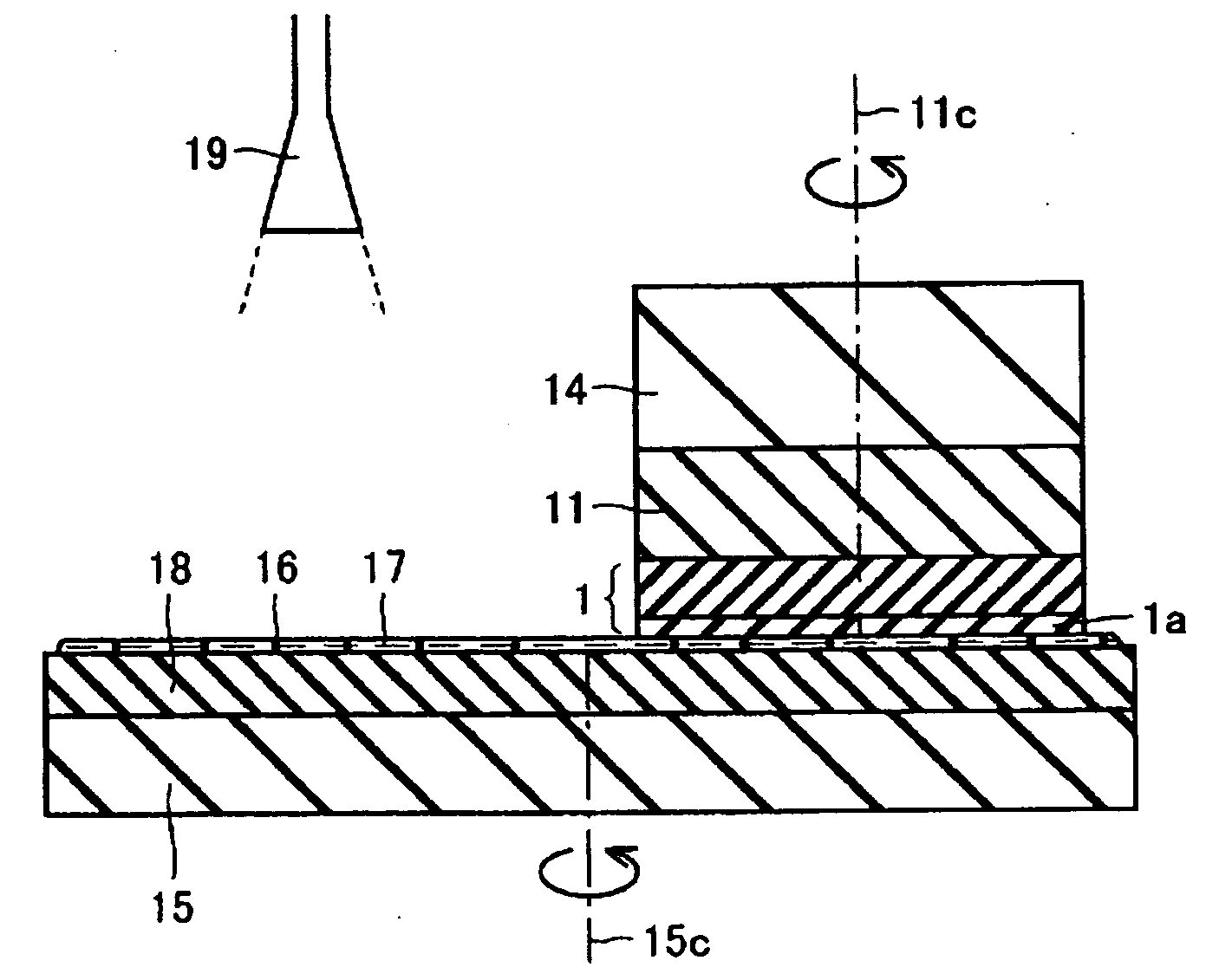
[0058] This example describes the case where a surface of a GaN crystal film grown by an HVPE method is mechanically lapped and then further polished.

[0059] (1-1) Growth of GaN Crystal Film

[0060] A GaN crystal film was grown by an HVPE method using a GaAs crystal substrate with a diameter of 50 mm as a base substrate. A boat containing metallic Ga was charged in a reacting furnace at atmospheric pressure and was heated to 800° C. A mixed gas of HCl gas and a carrier gas (H2 gas) was introduced into the boat to generate GaCl gas and a mixed gas of HN3 gas and a carrier gas (H2 gas) was introduced into the reacting furnace, thereby allowing to react the GaCl gas and the NH3 gas. Thus, a GaN crystal film having a thickness of 3 mm was grown on the base substrate (GaAs crystal substrate) disposed in the reacting furnace. In this step, the growth temperature of the GaN crystal film was 1,050° C., the partial pressure of the HCl gas in the reacting furnace was 2 kPa, and the partial pre...

example 2

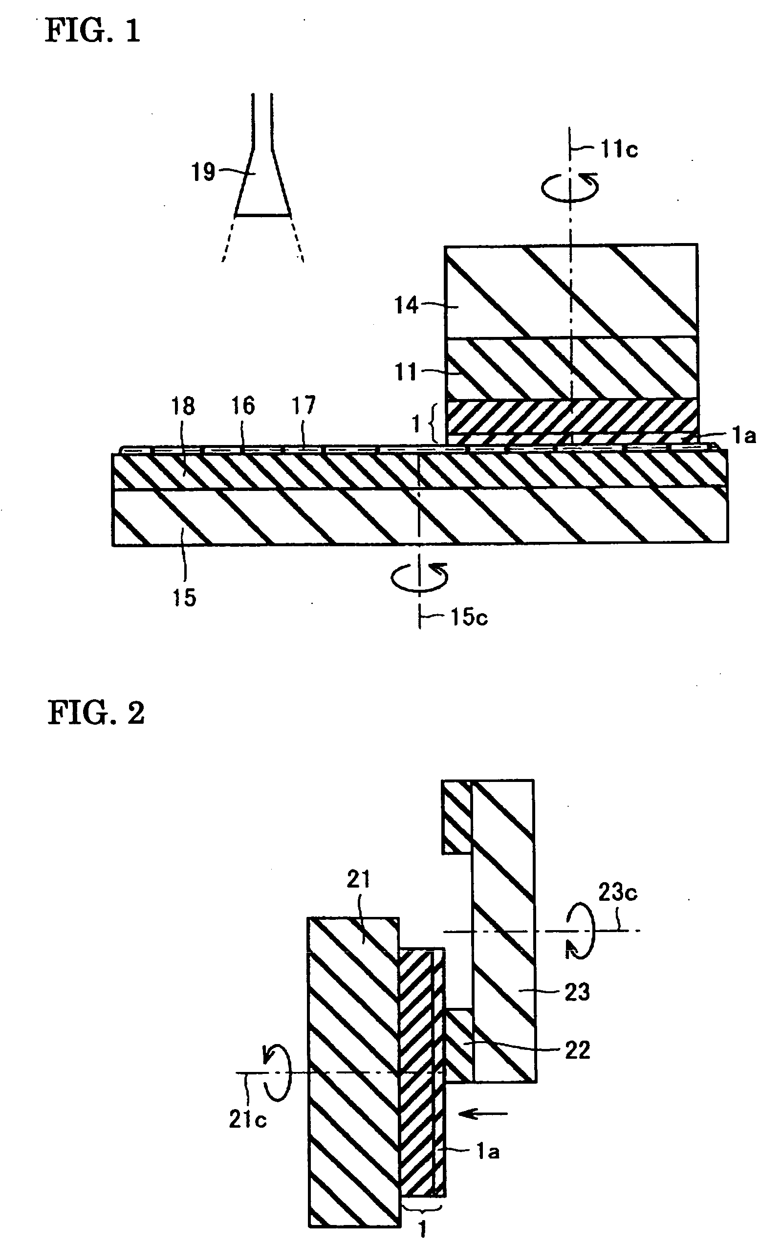
[0072] A surface treatment of a GaN crystal substrate was performed and an epitaxial layer was formed as in Example 1 except that an aqueous nitric acid solution containing colloidal silica (SiO2) having a grain size of 0.1 μm and serving as the abrasive grains 16 and trichloroisocyanuric acid (hereinafter referred to as TCIA) serving as an oxidizing agent wherein the pH was adjusted to 2.4 and the oxidation-reduction potential was adjusted to 1,420 mV was used as the polishing liquid 17. Table I summarizes the results.

examples 3 to 5

[0073] A surface treatment of a GaN crystal substrate was performed and an epitaxial layer was formed as in Example 1 except that an aqueous nitric acid solution containing Al2O3 particles serving as the abrasive grains 16 and TCIA serving as an oxidizing agent wherein the pH was adjusted to 3.5 and the oxidation-reduction potential was adjusted to 1,200 mV was used as the polishing liquid 17. The abrasive grains 16 having a grain size of 0.5 μm (Example 3), 1.0 μm (Example 4), or 2.0 μm (Example 5) were used. Table I summarizes the results.


PUM

PropertyMeasurementUnit
grain sizeaaaaaaaaaa
thicknessaaaaaaaaaa
surface roughnessaaaaaaaaaa

Abstract

A method of surface treatment of a Group III nitride crystal film includes polishing a surface of the Group III nitride crystal film, wherein a pH value x and an oxidation-reduction potential value y (mV) of a polishing liquid used for the polishing satisfy both relationships of y≧−50x+1,000 and y≦−50x+1,900.

Description

BACKGROUND OF THE INVENTION [0001] 1. Field of the Invention [0002] The present invention relates to a method of surface treatment of a Group III nitride crystal film used for substrates of semiconductor devices such as a light-emitting device, an electronic device, and a semiconductor sensor. Furthermore, the present invention relates to a Group III nitride crystal substrate prepared by the method of surface treatment of the Group III nitride crystal film. [0003] 2. Description of the Background Art [0004] Group III nitride crystals such as a GaN crystal and an AlN crystal are very useful materials for producing substrates of semiconductor devices such as a light-emitting device, an electronic device, and a semiconductor sensor. Herein, the term “Group III nitride crystals” refers to crystals composed of a Group III element and nitrogen, e.g., GaxAlyIn1-x-yN crystals (0≦x, 0≦y, and x+y≦1). [0005] A Group III nitride crystal substrate used as a substrate of a semiconductor device is...

Claims


Application Information

Patent Timeline
Patent Type & Authority Applications(United States)
IPC IPC(8): C30B25/00C30B23/00C30B28/12C30B28/14B24B37/00H01L21/304
CPCC09G1/02C30B29/403H01L2924/1305Y10T428/24355H01L2924/12041H01L2924/1306H01L2224/73265H01L2224/48247H01L2224/48091H01L24/32H01L2224/32245H01L2224/32257H01L33/32C30B33/00H01L21/02024C30B35/00H01L2924/00014H01L2924/00H01L2924/12042H01L2924/00012
Inventor ISHIBASHI, KEIJINISHIURA, TAKAYUKI
Owner SUMITOMO ELECTRIC IND LTD
Why Eureka
Try Eureka