

Semiconductor element, organic transistor, light-emitting device, and electronic device
- Summary
- Abstract
- Description
- Claims
- Application Information
AI Technical Summary
Benefits of technology
Problems solved by technology
Method used
Image

Examples
embodiment mode 1
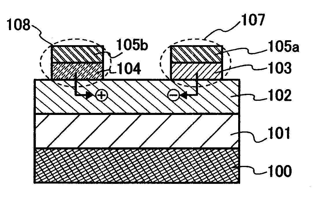
[0056] A semiconductor element which is an embodiment mode of the present invention will be explained by giving drawings illustrated in FIGS. 1A to 1C, FIGS. 2A to 2C, FIGS. 3A to 3D, FIG. 4, FIGS. 5A to 5C, FIGS. 6A to 6C, FIGS. 7A to 7D, and FIGS. 8A to 8D as examples.
[0057] A semiconductor element according to the present invention illustrated in FIG. 1A includes a first electrode 100, an insulating film 101, a semiconductor layer 102, a second electrode 107, and a third electrode 108.
[0058] The first electrode 100 is formed over an arbitrary insulator such as an insulating substrate or an insulating film which is not shown, and the insulating film 101 electrically insulates the semiconductor layer 102 and the first electrode 100. In addition, the second electrode 107 is formed of two layers of a conductive layer 105a and a layer 103 made of a second composite material and the third electrode 108 is formed of two layers of a conductive layer 105b and a layer 104 made of a first...
embodiment mode 2
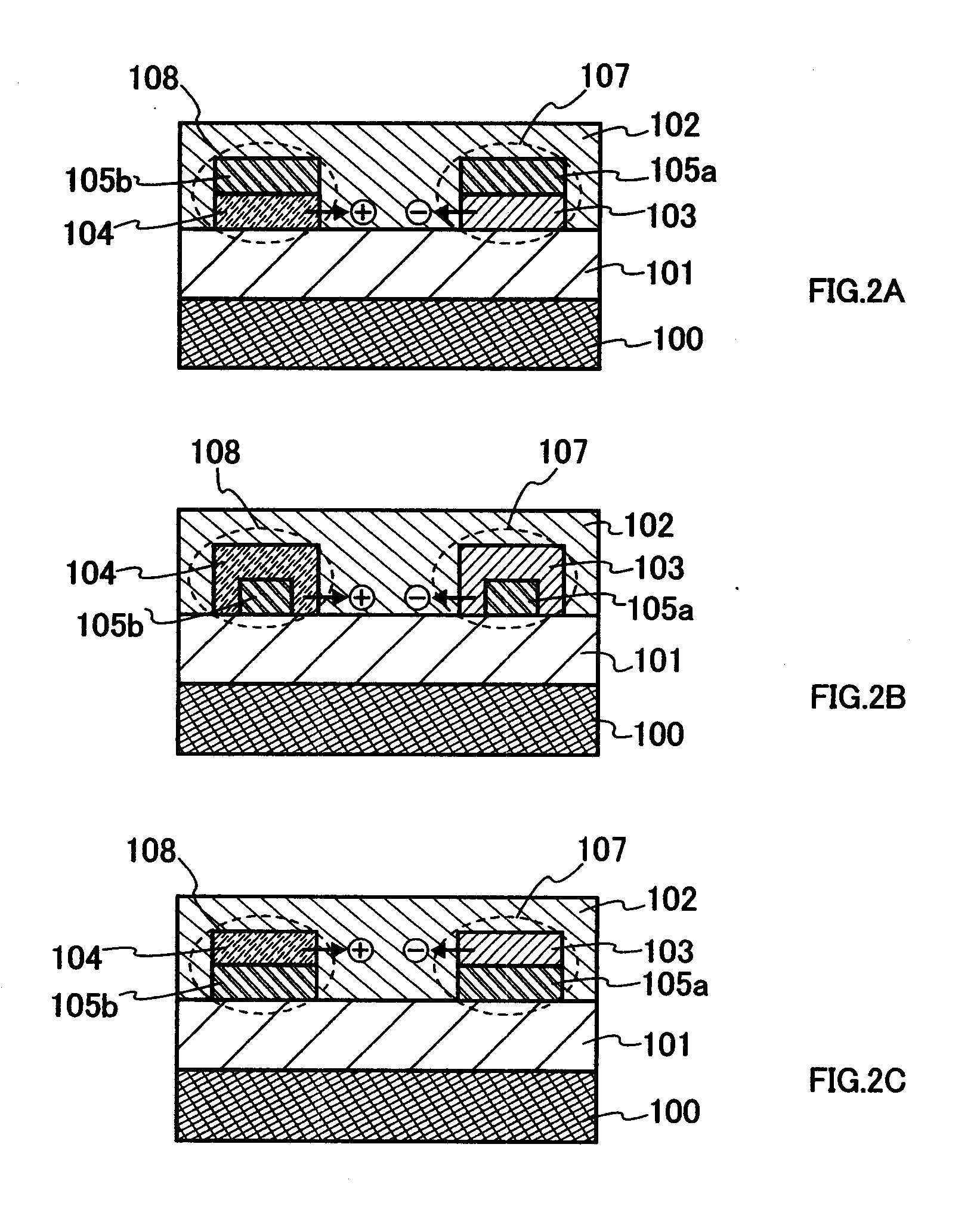
[0169] A semiconductor element according to the present invention having a structure different from those in FIGS. 1A to 1C, FIGS. 2A to 2C, FIGS. 3A to 3D, FIGS. 5A to 5C, FIGS. 6A to 6C, FIGS. 7A to 7D, and FIGS. 8A to 8D will be explained with reference to FIGS. 9A to 9C, FIGS. 10A to 10C, FIGS. 11A to 11C, and FIGS. 12A to 12C.
[0170] A semiconductor element according to the present invention each shown in FIGS. 9A to 9C includes a first electrode 100, an insulating film 101, a layer 106e having an electron-transporting property, a second electrode 107, a third electrode 108, and a semiconductor layer 102 and, in the basic structure, FIG. 9A, FIG. 9B, and FIG. 9C correspond to FIG. 2A, FIG. 3B, and FIG. 8B, respectively. The different portion in each corresponding structure is that the layer 106e having an electron-transporting property is formed between the insulating film 101 and each of the second electrode 107, the third electrode 108, and the semiconductor layer 102.
[0171]...
embodiment mode 3
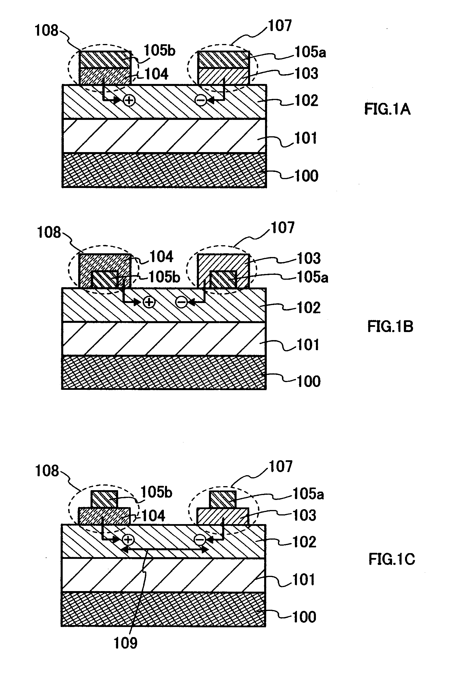
[0190] A method for manufacturing a semiconductor element according to the present invention will be explained with reference to FIGS. 13A to 13E by giving FIG. 2C as an example.
[0191] First, a first electrode 15 made of tungsten is deposited over a quartz substrate 16 in 100 nm thick, an insulating film 12 made of silicon dioxide (SiO2) is deposited over the first electrode 15 in 100 nm thick, and conductive layers 17a and 17b made of tungsten are deposited over the insulating film 12. After depositing tungsten over an entire surface of the substrate by a sputtering method or the like, a mask is formed by photolithography, and the first electrode 15 is etched in a desired shape. Either wet etching or dry etching may be used for the etching. The insulating film 12 is formed by a CVD method. In addition, the conductive layers 17a and 17b may be formed in the same manner as the first electrode 15. Moreover, over the conductive layer 17a, a layer 13a made of a second composite materia...
PUM
 Abstract
Description
Claims
Application Information