Semiconductor device and boost circuit

a technology of a booster circuit and a semiconductor device, which is applied in the direction of pulse generators, pulse techniques, instruments, etc., can solve problems such as the degradation of conversion efficiency, and achieve the improvement of the mobility of field-effect transistors, the high breakdown voltage of transistors, and the conversion efficiency.

Inactive Publication Date: 2006-10-26
SEIKO EPSON CORP
View PDF5 Cites 6 Cited by
  • Summary
  • Abstract
  • Description
  • Claims
  • Application Information

AI Technical Summary

Benefits of technology

[0007] An advantage of the invention is to provide a semiconductor device and a booster circuit that can improve the conversion efficiency at the time of voltage boosting, while maintaining a high breakdown voltage of transistors.
[0008] According to a first embodiment of the invention, a semiconductor device includes: a field-effect transistor that configures a charge-pump circuit; and a supporting substrate that supports the field-effect transistor so that the field-effect transistor provided on the supporting substrate becomes warpable in the channel direction.
[0009] With the above semiconductor device, a stress can be applied to the channel region of a field-effect transistor so as to warp the channel region of the field-effect transistor. Therefore, the mobility of a field-effect transistor can be improved and the transconductance of a field-effect transistor can also be increased, which makes it possible to reduce the internal impedance of a charge-pump circuit even in the case of using a high-breakdown-voltage transistor for the purpose of latchup prevention. As a result, the conversion efficiency at the time of voltage boosting can be improved and therefore various power supplies, including high-breakdown-voltage power supplies, can be embedded into semiconductor integrated circuits, while lowering the level of power supply voltage inside semiconductor integrated circuits.
[0010] Further, in the semiconductor device according to the first embodiment of the invention, it is preferable that the field-effect transistor includes: a semiconductor layer that is formed on the supporting substrate; a well that is formed on the semiconductor layer; a gate electrode that is provided on the well; a source layer that is provided on one side of the gate electrode and formed on the well; a drain layer that is provided on the other side of the gate electrode and formed on the well; and a backgate contact that is provided on the well and couples the well to the source layer.
[0011] With the above configuration, the well potential can be brought into accordance with the source potential, leading to an effective latchup prevention even in the case where N-channel field-effect transistors and P-channel field-effect transistors coexist on the same substrate.
[0012] Further, according to a second embodiment of the invention, a booster circuit includes: a first N-channel field-effect transistor, wherein a first pulse is inputted to a gate; a first P-channel field-effect transistor that is serially coupled to the first N-channel field-effect transistor, wherein the first pulse is inputted to a gate; a second N-channel field-effect transistor, wherein a gate is coupled to a drain of the first N-channel field-effect transistor; a second P-channel field-effect transistor that is serially coupled to the second N-channel field-effect transistor; a third N-channel field-effect transistor, wherein a second pulse, which has the opposite phase to the first pulse, is inputted to a gate and a source is coupled to a drain of the second N-channel field-effect transistor; a third P-channel field-effect transistor that is serially coupled to the third N-channel field-effect transistor, wherein a source is coupled to a source of the second N-channel field-effect transistor and the second pulse is inputted to a gate; a fourth N-channel field-effect transistor wherein a gate is coupled to a drain of the third N-channel field-effect transistor and a source is coupled to a source of the second N-channel field-effect transistor; a fourth P-channel field-effect transistor that is serially coupled to the fourth N-channel field-effect transistor, wherein: a gate is coupled to a drain of the third P-channel field-effect transistor, a source is coupled to the source of the third P-channel field-effect transistor, and a drain is coupled to a source of the first P-channel field-effect transistor; a first capacitor that is coupled to the drain of the second N-channel field-effect transistor, whereto the first pulse is inputted; a second capacitor that is coupled to a drain of the fourth N-channel field-effect transistor, whereto the second pulse is inputted; and a supporting substrate, on which the first to fourth N-channel field-effect transistors; the first to fourth P-channel field-effect transistors; and the first and second capacitors are provided, that supports the first to fourth N-channel field-effect transistors and the first to fourth P-channel field-effect transistors so that each of the first to fourth N-channel field-effect transistors and the first to fourth P-channel field-effect transistors becomes warpable in the channel direction.

Problems solved by technology

Since such a configuration raises the internal impedance of a charge-pump circuit, there has been a problem of the degradation of conversion efficiency.

Method used


Image

  • Semiconductor device and boost circuit
  • Semiconductor device and boost circuit
  • Semiconductor device and boost circuit

Examples


first embodiment

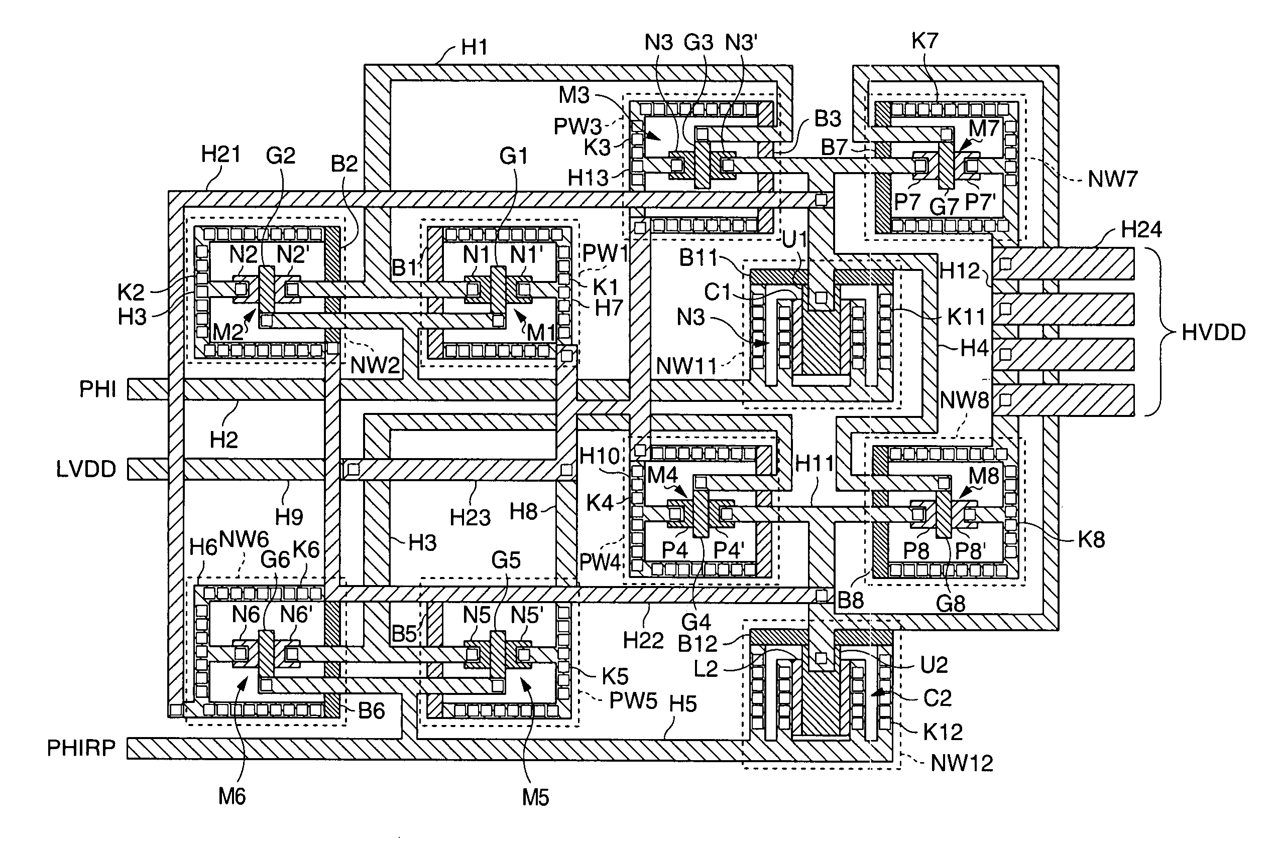
[0025]FIG. 1 is a circuit diagram showing an example configuration of a booster circuit to which the invention is applied.

[0026] In FIG. 1, the source of an N-channel field-effect transistor M1 is coupled to an LDVV terminal; and the source of a P-channel field-effect transistor M2 is coupled to a VDDORP terminal. Further, the drain of the N-channel field-effect transistor M1 and the drain of the P-channel field-effect transistor M2 are coupled to a PHIA terminal. Furthermore, the gate of the N-channel field-effect transistor M1 and the gate of the P-channel field-effect transistor M2 are coupled to a PHI terminal. In the foregoing configuration, the substrate potential of the N-channel field-effect transistor M1 is coupled to the source of the N-channel field-effect transistor M1; and the substrate potential of the P-channel field-effect transistor M2 is coupled to the source of the P-channel field-effect transistor M2.

[0027] Also, the source of an N-channel field-effect transisto...

second embodiment

[0051]FIG. 5 is a diagram showing a method for warping a field-effect transistor according to the invention.

[0052] In FIG. 5, a field-effect transistor T has a gate electrode G, as well as a source layer S and a drain layer D, which sandwich the gate electrode G. Further, a source contact C1 and a drain contact C2 are respectively formed on the source layer S and the drain layer D. Furthermore, the field-effect transistor T is mounted on a film substrate F so that the channel direction of the field-effect transistor T accords with the warpage direction of the film substrate F.

[0053] In the above configuration, by warping the film substrate F, the channel region of the field-effect transistor T can be warped, which improves the mobility of the field-effect transistor T. Therefore, the transconductance of the field-effect transistor T can also be increased, which makes it possible to reduce the internal impedance of a charge-pump circuit even in the case of using a high-breakdown-vol...


PUM


Abstract

A semiconductor device, includes: a field-effect transistor that configures a charge-pump circuit; and a supporting substrate that supports the field-effect transistor so that the field-effect transistor provided on the supporting substrate becomes warpable in a channel direction.

Description

[0001] Applicant hereby claims priority from JP 2005-081152 filed on Mar. 22, 2005, which is hereby incorporated by reference in its entirety. BACKGROUND [0002] 1. Technical Field [0003] The present invention relates to a semiconductor device and a booster circuit. In particular, the invention relates to a device that is applied to a method for improving the mobility of transistors used in a charge-pump circuit. [0004] 2. Related Art [0005] Along with the progress of semiconductor manufacturing process in recent years, the denser integration and more function multiplication of semiconductor integrated circuits have been being accelerated, and the power supply voltage inside a semiconductor integrated circuit has been becoming lower. In addition, accompanied by the more function multiplication of semiconductor integrated circuits, the embedding of various power supplies, including high-voltage power supplies, has also been increasing. For example, non-volatile memories such as flash ...

Claims


Application Information

Patent Timeline
Patent Type & Authority Applications(United States)
IPC IPC(8): H03K19/00
CPCH01L27/0222H01L27/105H02M3/07H01L29/7842H01L29/78603H01L29/7833
Inventor AJIKI, YOSHIHARU
Owner SEIKO EPSON CORP
Why Eureka
Try Eureka