Method for manufacturing semiconductor device

a manufacturing method and semiconductor technology, applied in the direction of semiconductor devices, electrical appliances, transistors, etc., to achieve the effect of reducing the generation of junction leakage current, and reducing the sheet resistance of the silicide layer

Active Publication Date: 2006-10-26
RENESAS ELECTRONICS CORP
View PDF5 Cites 37 Cited by
  • Summary
  • Abstract
  • Description
  • Claims
  • Application Information

AI Technical Summary

Benefits of technology

[0036] According to the above-described aspect of the present invention, in the lamp annealing apparatus including the temperature measurement unit that is capable of optically measuring a temperature of the silicon substrate, the temperature of the silicon substrate is elevated to the first temperature, at which a temperature measurement of the silicon substrate having the layer of cobalt deposited thereon is enabled to be conducted, and then, the temperature of the silicon substrate is held at around the first temperature to stabilize the temperature of the silicon substrate. Employing the silicon substrate which accumulated with the surface of the substrate with cobalt can reduce the temperature, at which the temperature measurement of the silicon substrate is enabled to be conducted with the temperature measurement unit, as compared with the case of employing the silicon substrate having the unprocessed surfaces. Having such configuration, the operation of holding the temperature of silicon substrate can be carried out according to a substantially flat temperature profile that does not exceed the temperature, at which an unusual reaction is induced between cobalt and silicon. Therefore, the obtained sheet resistance of the silicide layer is reduced, and further, any silicide-spike or cohesion is not generated in the diffusion layer, leading to an inhibition in the generation of the junction leakage current.
[0037] According to the present invention, a method for manufacturing a semiconductor device is provided, which promotes a reduced sheet resistance of a silicide layer and further a reduced generation of the junction leakage current.

Problems solved by technology

However, when the furnace annealing apparatus is employed, technical issues such as an increased sheet resistance of the cobalt silicide layer, an enhancement of a junction leakage current and the like are arisen.
It has been found that these issues as described above are correspondingly created even in a case of employing a lamp annealing apparatus that can achieve faster temperature ramp rate.

Method used


Image

  • Method for manufacturing semiconductor device
  • Method for manufacturing semiconductor device
  • Method for manufacturing semiconductor device

Examples


first embodiment

[0054] In the present embodiment, an exemplary implementation of employing a silicon wafer as the silicon substrate will be described. FIG. 8 is a flow chart, showing a procedure for manufacturing a semiconductor device in the present embodiment. The silicide layer is formed on the silicon substrate such as silicon wafer and the like according to the procedure of FIG. 8, so that semiconductor devices having a predetermined device such as transistor and the like can be manufactured by employing this procedure.

[0055] A procedure for manufacturing of FIG. 8 includes the following steps;

[0056] step 101: sputter;

[0057] step 102: first sintering;

[0058] step 103: unloading wafer;

[0059] step 104: removing unreacted Co; and

[0060] step 105: second sintering.

[0061]FIG. 9 is also a flowchart, showing a part of the manufacturing procedure shown in FIG. 8, and more specifically, describing the step 101 and the step 102 in detail. FIG. 12 is a graph, showing a temperature profile of the sil...

second embodiment

[0095] In the present embodiment, the manufacture of the transistor by employing the process for manufacturing the semiconductor device described in first embodiment will be further described in more detail. While an exemplary implementation of forming a complementary metal oxide semiconductor field effect transistor (CMOSFET) on a silicon substrate is described, conductivity type and number of transistor(s) are not particularly limited, and a predetermined number of transistor(s) having respective predetermined conductivity type(s) may be provide on the silicon substrate.

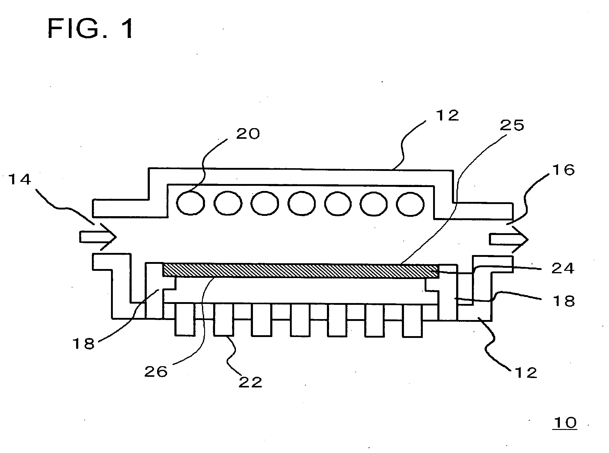
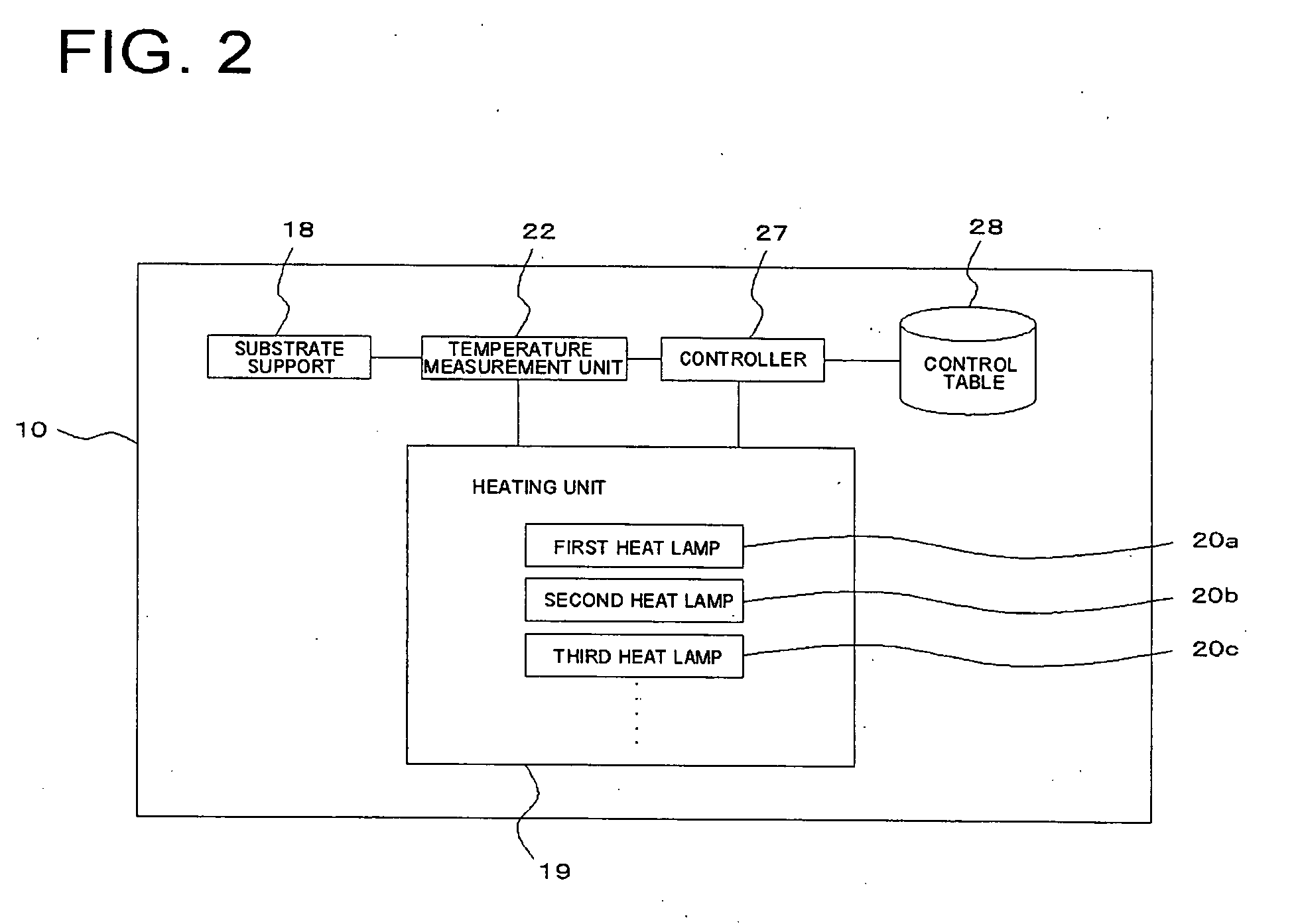
[0096] First of all, a configuration of lamp annealing apparatus of the present embodiment will be described on the basis of a schematic cross-sectional view in FIG. 1 and a functional block diagram of FIG. 2.

[0097] As shown in FIG. 1 and FIG. 2, a lamp annealing apparatus 10 includes: a chamber 12 for containing a silicon substrate 24 having cobalt deposited thereon; a plurality of heat lamps 20 provided in the ...

examples

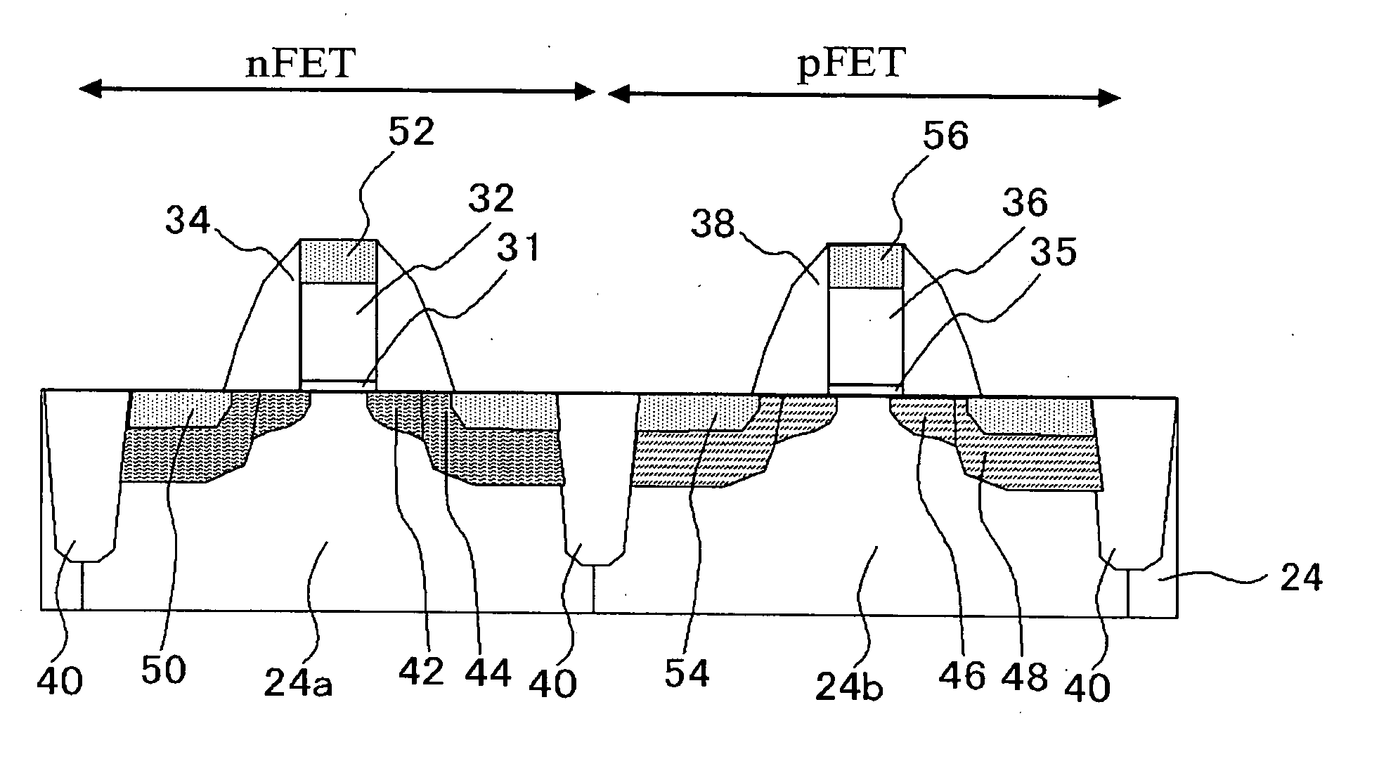
[0186] In the present example, a p-type FET (FIG. 4) was formed in a silicon substrate by employing a method described in first embodiment.

[0187] The configuration of a side of a p-type FET shown in FIG. 3 was formed in a silicon substrate 24, and then, Co was sputtered on the entire device-forming surface in a sputter apparatus at a temperature of 350 degree C. Thereafter, the silicon substrate was transferred into a lamp annealing apparatus, where first sintering processing was conducted. In the first sintering, the silicon substrate was once elevated to a temperature of 300 degree C., and then, the temperature was held at 300 degree C. for 10 seconds, which was a temperature holding operation. Thereafter, temperature-elevating operations were conducted from 300 degree C. to 700 degree C. at various temperature ramp rate. Then, the temperature was held at 700 degree C. for 60 seconds to form CoSi layer on the device-forming surface. After the first sintering, unreacted Co was rem...


PUM

PropertyMeasurementUnit
junction depthsaaaaaaaaaa
temperatureaaaaaaaaaa

Abstract

Method for manufacturing a semiconductor device, includes: forming a layer of dicobalt monosilicide (Co2Si) or of cobalt (Co) on a device-forming surface of a silicon substrate in a sputter apparatus, by utilizing a predetermined temperature profile; elevating a temperature of the silicon substrate to a predetermined temperature T2, which is equal to or higher than 600° C., conducted after forming the layer of Co or Co2Si; and forming a layer of monocobalt monosilicide (CoSi) on the device-forming surface of the silicon substrate at a temperature equal to or higher than T2, conducted after heating the silicon substrate to T2, wherein, the silicon substrate is elevated to a temperature between a highest reachable temperature T1 of the silicon substrate during forming the layer of Co or Co2Si and the temperature T2 at a temperature ramp rate of equal to or higher than 50° C./sec.

Description

[0001] This application is based on Japanese patent application No. 2005-127,107 and Japanese patent application No. 2006-108,914, the contents of which are incorporated hereinto by reference. BACKGROUND [0002] 1. Technical Field [0003] The present invention relates to a method for manufacturing a semiconductor device comprising a layer of cobalt silicide. [0004] 2. Related Art [0005] Among conventional methods for manufacturing semiconductor devices, a method for manufacturing a semiconductor device having a layer of titanium silicide formed on a silicon substrate is typically described in Japanese Patent Laid-Open No. H10-256,191 (1998). Resistances in electrodes such as a gate or source / drain can be reduced by providing the titanium silicide layer, like the above-described configuration. In recent years, a layer of cobalt silicide is employed, in place of a layer of titanium silicide, according to requirements for achieving faster operation of a device. Such cobalt silicide layer...

Claims


Application Information

Patent Timeline
Patent Type & Authority Applications(United States)
IPC IPC(8): H01L21/44
CPCH01L21/28052H01L21/28518H01L29/7833H01L29/665H01L29/6659H01L21/324
Inventor MATSUDA, TOMOKOITOU, TAKAMASA
Owner RENESAS ELECTRONICS CORP
Why Eureka
Try Eureka