Optical recording medium
a recording medium and optical recording technology, applied in the field of rewritable optical recording medium, can solve the problems of limiting the crystallization speed, the difficulty of achieving high-speed recording corresponding to 6, and the use of dvds using gasb binary alloys, etc., and achieves the effect of small reduction of reflectan
- Summary
- Abstract
- Description
- Claims
- Application Information
AI Technical Summary
Benefits of technology
Problems solved by technology
Method used
Image
Examples
examples
[0093] Hereinafter, the invention will be illustrated more specifically with reference to several examples and comparative examples. However, the invention is not limited to these examples and / or the used initialization device, etc. For example, the invention is also applicable to a surface recording type rewritable optical recording medium in which layers are formed in the reverse order, or to a recording medium in which two same or different optical recording media are laminated to each other via a resin protective layer instead of a substrate for laminating used in an optical recording medium of DVD system.
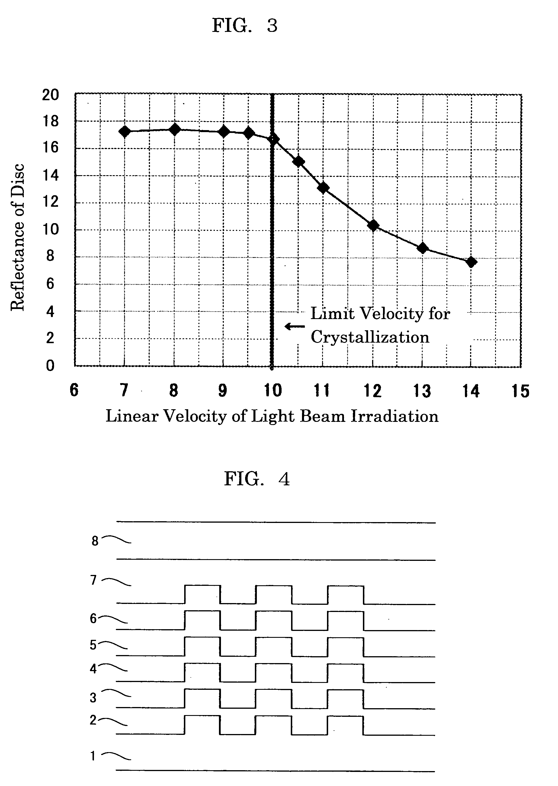
[0094]FIG. 4 shows a schematic cross-sectional view of a phase-change optical disc (hereinafter, may be referred to as “optical disc”), which is an example of the rewritable optical recording medium of the invention. This optical disc comprises a transparent substrate 1 on which a guide groove to guide a laser beam is provided, a first protective layer 2, a phase-change record...
examples 1 to 6
[0095] A substrate 1 was a substrate made of polycarbonate with a diameter of 12 cm and a thickness of 0.6 mm, and having a guide groove with a tracking pitch of 0.74 μm. A first protective layer 2 was a 65 nm thick layer containing ZnS (80 mole %)-SiO2 (20 mole %). A phase-change recording layer 3 was a 16 nm thick layer containing Ga11Sb83Sn6 (Example 1), Ga14Sb58Sn28 (Example 2), Ga12Sb83Sn5 (Example 3), Ga10Sb89Sn1 (Example 4), Ga11Sb86Sn3 (Example 5), or Ga11Sb84Sn5 (Example 6). A second protective layer 4 was a 14 nm thick layer containing ZnS (80 mole %)-SiO2 (20 mole %). A third protective layer 5 was a 4 nm thick layer containing SiC. A reflective layer 6 was a 140 nm thick layer containing Ag. A substrate 8 for laminating was a substrate made of polycarbonate with a diameter of 12 cm and a thickness of 0.6 mm, which were the same as those of the substrate 1.
[0096] Initially, on the substrate 1, the first protective layer 2, phase-change recording layer 3, second protectiv...
example 7
[0106] An optical disc having the same layer configuration as that of the optical disc of Example 3 was prepared in the same way as in Example 3, except that the material of phase-change recording layer 3 was changed to Ga11Sb59Sn22Ge8. Compared with Example 3, in this Example, a phase-change material was used in which the ratios of Ga and Sb were reduced, but instead, to which Ge, effective for storage reliability, and Sn, making the crystallization speed faster, were added.
[0107] This optical disc was evaluated after initialization in the same way. It was found that satisfactory recording properties was obtained as in Example 3, and further found that the archival property hardly deteriorated. Results are shown in Table 1.
PUM
| Property | Measurement | Unit |
|---|---|---|
| thickness | aaaaa | aaaaa |
| thickness | aaaaa | aaaaa |
| thickness | aaaaa | aaaaa |
Abstract
Description
Claims
Application Information


