Apparatus, precursors and deposition methods for silicon-containing materials

a technology of silicon-containing materials and precursors, applied in the direction of liquid/solution decomposition chemical coating, superimposed coating process, resistive material coating, etc., can solve the problems of rc delay becoming the dominant factor, and the problem of integrating polymeric porous materials into semiconductor device manufacturing flows

Active Publication Date: 2006-11-02
ASM JAPAN
View PDF54 Cites 232 Cited by
  • Summary
  • Abstract
  • Description
  • Claims
  • Application Information

AI Technical Summary

Problems solved by technology

For modern sub-micron technology, however, the RC delay has become the dominant factor.
However, the integration of polymeric porous materials into s

Method used


Image

  • Apparatus, precursors and deposition methods for silicon-containing materials
  • Apparatus, precursors and deposition methods for silicon-containing materials
  • Apparatus, precursors and deposition methods for silicon-containing materials

Examples


examples

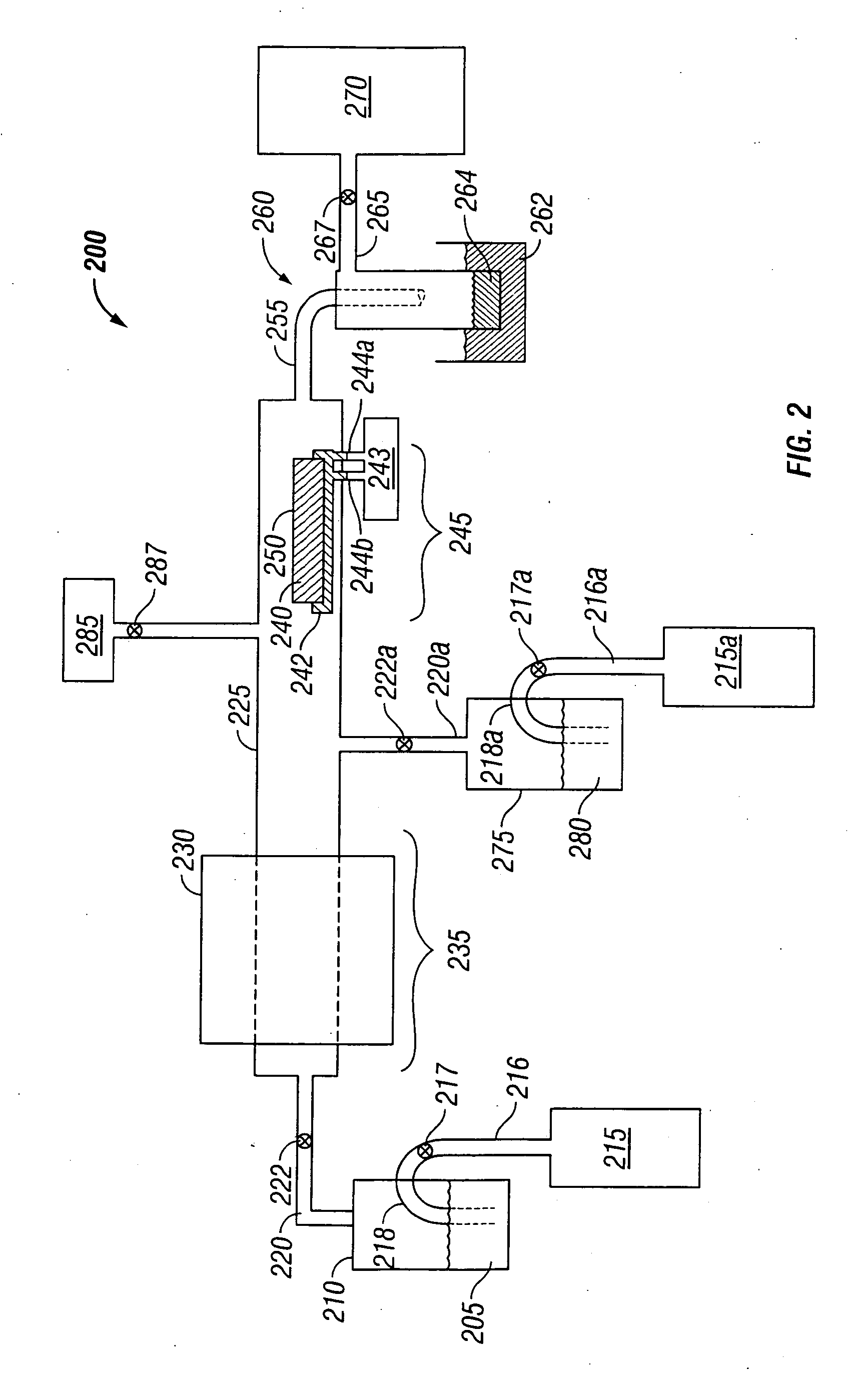
[0084] Depositions described in the Examples below were carried out using a deposition system of the general design illustrated in FIG. 2. The system was cleaned and thoroughly dried using heating and pumping overnight under vacuum (diffusion pump, nominal vacuum 10−5 Torr) using a cold trap (liquid nitrogen, about −196° C.) prior to deposition. During deposition, the precursor was fed by unimpeded direct vapor draw at the nominal pressure applied by the diffusion pump, the temperature in the hot zone was about 725° C., and the cold trap was maintained at about −196° C., unless otherwise stated. Si-precursor, porogen, substrate temperature, and annealing conditions were varied as described below.

examples 1-2

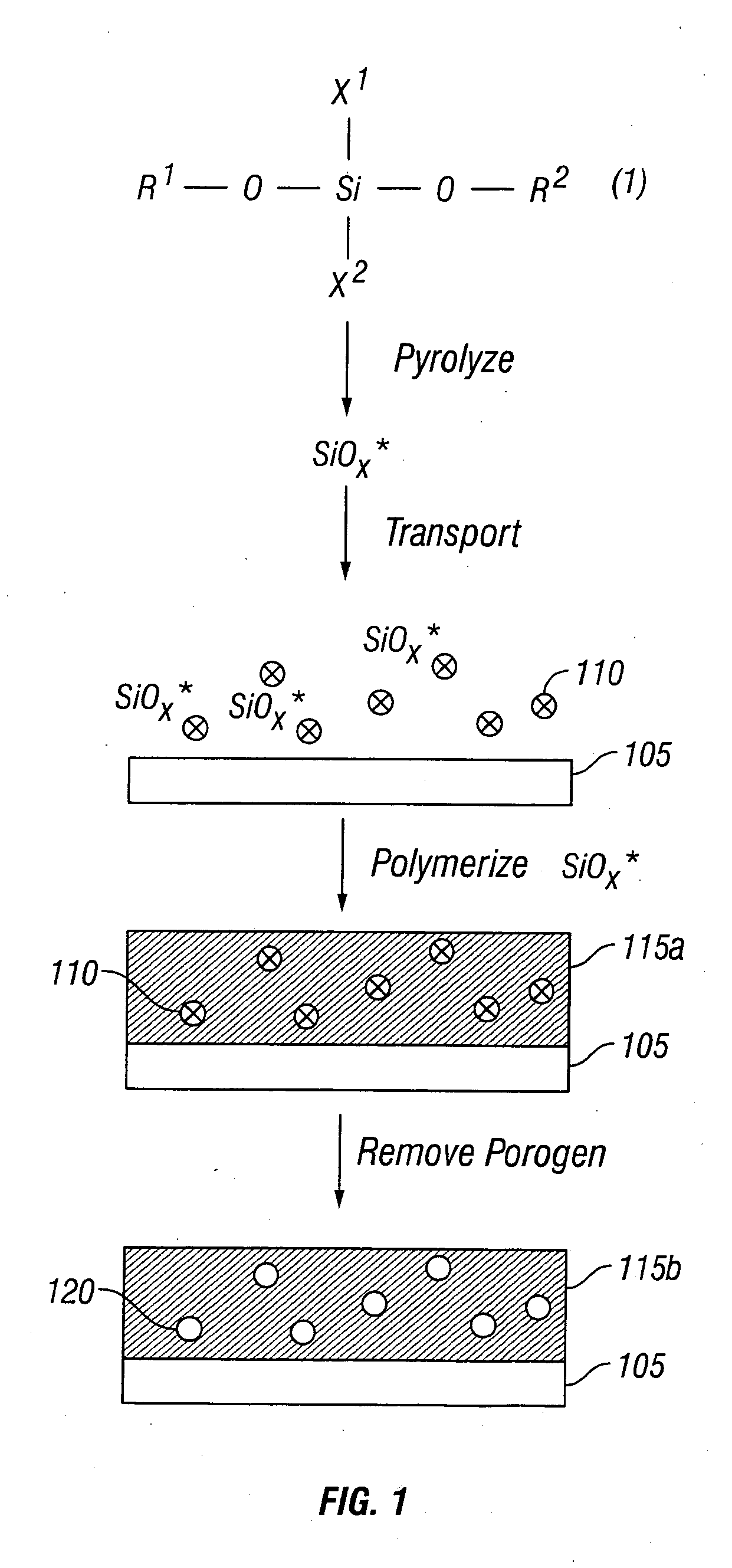
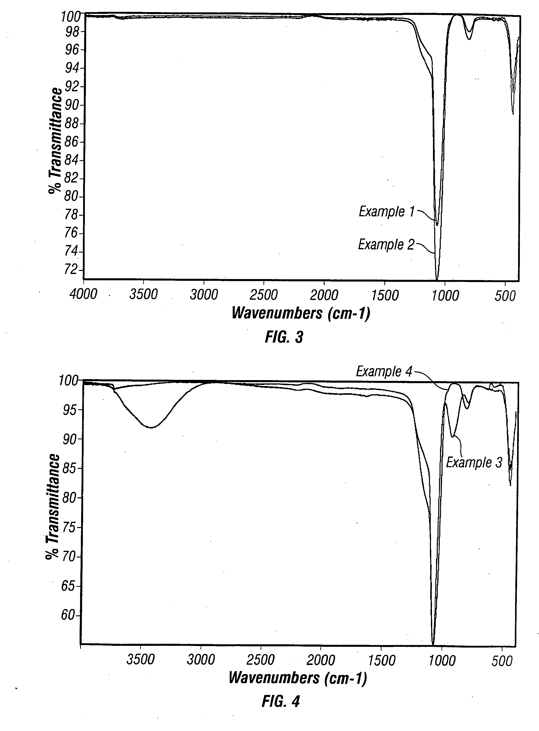
[0085] Two Si-containing films were deposited using bis-tertiarybutoxy dichlorosilane of the formula (IV). No porogen was used. The substrate temperature was about 0° C. By-product Cl—C(CH3)3 was isolated from the cold trap, indicating that SiOx* was formed and subsequently polymerized to form the Si-containing film (comprising —(SiO2)— recurring units) in a manner similar to that illustrated in Scheme (A) for bis-tertiarybutoxy dibromosilane. After deposition, both films were exposed to air for several days. The films were then thermally annealed at 420° C. for one hour under either air (Example 1) or nitrogen (Example 2). The resulting Si-containing films were characterized by infrared spectroscopy (FTIR) as shown in FIG. 3. The FTIR spectra shown in FIG. 3 confirm that the deposited film was a three-dimensional network of silicon and oxygen atoms comprising —(SiO2)— recurring units.

examples 3-4

[0086] A Si-containing film was deposited using bis-tertiarybutoxy dibromosilane of the formula (III). No porogen was used. The substrate temperature was about 0° C. By-product Br—C(CH3)3 was isolated from the cold trap, indicating that SiOx* was formed and subsequently polymerized to form the Si-containing film (comprising —(SiO2)— recurring units as illustrated in Scheme (A)). The resulting Si-containing film was characterized by FTIR before annealing (Example 3) and after annealing at 400° C. for one hour under vacuum (Example 4) as shown in FIG. 4. The FTIR spectra shown in FIG. 4 confirm that both of the films were three-dimensional networks of silicon and oxygen atoms comprising —(SiO2)— recurring units. The spectra also show that the as-deposited film (Example 3) contained Si—OH bonds after exposure to air as indicated by the Si—OH stretching-bending mode observed near 925 cm−1, and that annealing under vacuum (Example 4) changed the structure of the film by reducing the amou...


PUM

PropertyMeasurementUnit
Temperatureaaaaaaaaaa

Abstract

A method for making a Si-containing material comprises transporting a pyrolyzed Si-precursor to a substrate and polymerizing the pyrolyzed Si-precursor on the substrate to form a Si-containing film. Polymerization of the pyrolyzed Si-precursor may be carried out in the presence of a porogen to thereby form a porogen-containing Si-containing film. The porogen may be removed from the porogen-containing Si-containing film to thereby form a porous Si-containing film. Preferred porous Si-containing films have low dielectric constants and thus are suitable for various low-k applications such as in microelectronics and microelectromechanical systems.

Description

BACKGROUND OF THE INVENTION [0001] 1. Field of the Invention [0002] This application relates generally to the deposition of silicon-containing materials in semiconductor and microelectromechanical systems (MEMS) processing. More particularly, this application relates to the production of activated Si precursors and to the polymerization of those precursors to form Si-containing films. [0003] 2. Description of the Related Art [0004] In recent years, microelectronics manufacturers have been shrinking transistor size in integrated circuits (IC's) to improve device performance. This has resulted in increased speed and device density. The speed of an electrical signal in an IC is primarily governed by two components—the switching time of an individual transistor, known as transistor gate delay, and the signal propagation time between transistors, known as RC delay. In past years, the RC delay was negligible in comparison with the signal propagation delay. For modern sub-micron technology...

Claims


Application Information

Patent Timeline
IPC IPC(8): C08G77/00B32B3/26B32B3/00
CPCC09D4/00C09D183/04C23C16/401C08G77/04Y10T428/249953Y10T428/249969
Inventor TODD, MICHAEL A.
Owner ASM JAPAN
Why Eureka
Try Eureka