Anisotropic electrically conductive film and method of producing the same

a technology of electrically conductive film and anisotropic conductive film, which is applied in the direction of mechanical vibration separation, electronic vibration separation, instruments, etc., can solve the problems of inability to use porous film thus formed, buckled electrically conductive metal lump, and inability to make elastic recovery when compressive load, etc., to achieve elastic recovery, low compression load, and suitable for repeated use

Inactive Publication Date: 2006-11-09
SUMITOMO ELECTRIC IND LTD
View PDF8 Cites 14 Cited by
  • Summary
  • Abstract
  • Description
  • Claims
  • Application Information

AI Technical Summary

Benefits of technology

[0008] An object of the present invention is to provide anisotropic conductive films which are mainly used for an inspection of semiconductor wafers and which are elastic in the film thickness direction so that conductiveness in the film thickness direction can be afforded with a low compression load. Another object of the present invention is to provide anisotropic conductive films in which the sizes and pitches of conductive parts can be made finer.
[0011] Therefore, the anisotropic conductive film of the present invention has elastic recovery property upon compression as well as elasticity, not only in the base film but also in the conductive parts, and can be applied to repeated use. Also, the anisotropic conductive film of the present invention can be made conductive in the film thickness direction at a low compression load. Moreover, in the anisotropic conductive film of the present invention, the conductive parts and pitches between the conductive parts can be made finer. Thus, the present invention has been completed based on such discovery and knowledge.
[0035] According to the present invention, it is possible to provide an anisotropic conductive film which has elasticity in the film thickness direction and in which conduction can be afforded in the film thickness direction with a low compression load, and moreover which is capable of elastic recovery and suitable for repeated use. Also, an anisotropic conductive film in which the sizes and pitches of the respective conductive parts can be made finer is provided according to the present invention. The anisotropic conductive film of the present invention is capable of exhibiting electrical continuity in the film thickness direction with a low compression load, and is an anisotropic conductive film mainly suitable for an inspection of semiconductor wafers and the like, and moreover even with repeated application of load, the film thickness thereof can recover because of elasticity, thereby allowing repeated use for the inspection.

Problems solved by technology

However, in the case of the porous film having conductive parts provided by filling conductive metal in the porous structure of specific parts thereof, the electrically conductive metal lump buckles and does not make elastic recovery when a compressive load is applied.
Therefore, the porous film thus formed cannot be used repeatedly.

Method used


Image

  • Anisotropic electrically conductive film and method of producing the same
  • Anisotropic electrically conductive film and method of producing the same
  • Anisotropic electrically conductive film and method of producing the same

Examples


example 1

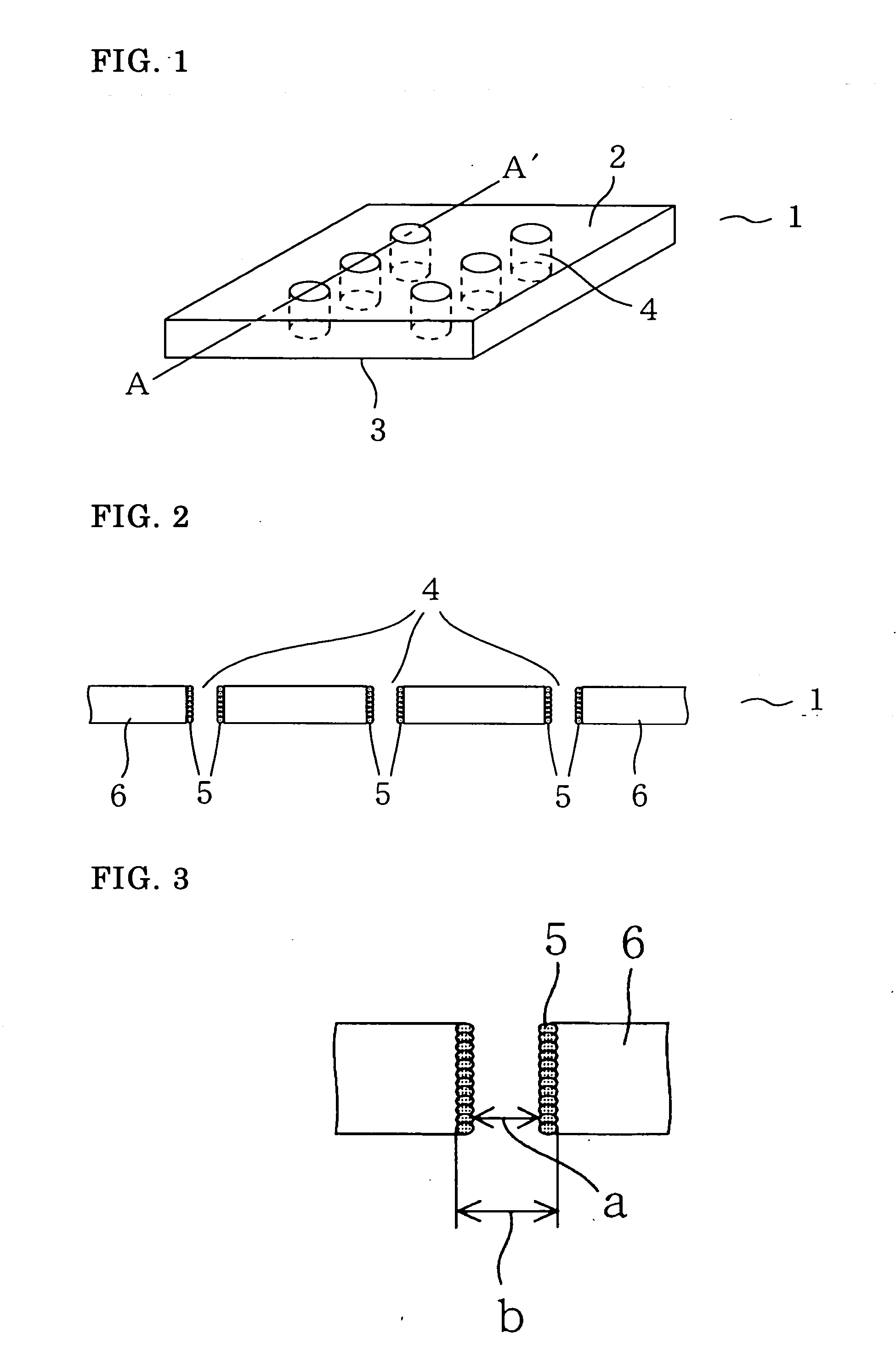
[0095] Three sheets of porous PTFE films made by an expansion method and having an area of 10 cm square, a porosity of 60%, a mean hole diameter of 0.1 μm (BP=150 kPa), and a film thickness of 30 μm were laminated and put between two stainless boards having a thickness of 3 mm, a longitudinal length of 150 mm and a width of 100 mm, and they were subjected to heat treatment at a temperature of 350° C. for 30 minutes under the load of the stainless board. After the heating, they were subjected to quenching by water provided on the stainless board so that a fusion-bonded three layer laminated body of porous PTFE film was obtained.

[0096] Subsequently, a tungsten sheet, in which openings were formed at uniform sequences by an opening area ratio of 9%, at an opening diameter of 15 μmφ, and at a pitch of 80 μm, was placed on one side of the laminated body and an irradiation of synchrotron radiation rays was performed so that through holes were formed in the film thickness direction and eq...

example 2

[0103] A laminated body was formed by fusion-bonding three porous PTFE films in the same method and conditions as Example 1. Through holes of 10 μmφ were formed in the laminated body, and a pre-treatment for plating was performed. After the delamination of mask layers, a base film was immersed for 20 minutes in an electroless copper plating solution while the solution was stirred sufficiently by air agitation, and copper particles were adhered only to the wall surfaces of the through holes of 10 μmφ so that conductiveness was afforded (the outer diameter of an electrode=17 μm). Subsequently, the same antirust treatment as in Example 1 was performed. Thus, an anisotropic conductive film including the base film that was a porous PTFE film made by the expansion method was obtained. When the same test as Example 1 was performed using the anisotropic conductive film, the conduction commencement load pressure was 6 kPa. After weight loading and non-weight loading were repeated 10 times wi...


PUM

PropertyMeasurementUnit
wavelengthaaaaaaaaaa
particle diameteraaaaaaaaaa
porosityaaaaaaaaaa

Abstract

The present invention is directed to an anisotropic conductive film and manufacturing methods thereof, in which an electrically insulative porous film made of synthetic resin is used as a base film and in which conductive parts capable of being provided with conductiveness in the film thickness direction are formed independently at plural positions of the base film by adhering conductive metal to resinous parts of porous structure in such a manner as piercing through from a first surface to a second surface.

Description

TECHNICAL FIELD [0001] The present invention relates to an anisotropic conductive film and the manufacturing method thereof, and more particularly to an anisotropic conductive film suitable for use in the burn-in test of semiconductor devices and the manufacturing method thereof. BACKGROUND ART [0002] A burn-in test is performed as one of screening techniques for removing an initial failure of semiconductor devices. In the burn-in test, accelerated stress that is higher in temperature and pressure than that of the operation condition of the semiconductor devices is applied, thereby accelerating the occurrence of failures so that defective products can be removed in a short time. For example, a number of semiconductor devices that have been packaged are arranged on a burn-in board, and a supply voltage and input signal to be accelerated stress are applied in a high temperature bath for a given time. Thereafter, the semiconductor devices are removed outside, and judgment tests are per...

Claims


Application Information

Patent Timeline
Patent Type & Authority Applications(United States)
IPC IPC(8): B32B3/00G01R1/04G01R31/28H01L21/48H01L23/482H01L23/498H01R43/00H05K3/40
CPCG01R1/0408G01R31/2863H01L21/486H01L23/4828H01L23/49827Y10T428/24917H01R43/007H05K3/4069H01L2924/0002H01L2924/09701H01L2924/00H01R11/01H01L21/52
Inventor MASUDA, YASUHITOOKUDA, YASUHIROHAYASHI, FUMIHIROHAGA, TSUYOSHI
Owner SUMITOMO ELECTRIC IND LTD
Why Eureka
Try Eureka