Semiconductor device and manufacturing method thereof
a technology of semiconductor devices and semiconductor films, applied in semiconductor devices, semiconductor/solid-state device details, electrical devices, etc., can solve the problems of abnormal growth of crystal defects, abnormal growth of silicide films, etc., to prevent abnormal growth and coagulation, increase junction leakage, and prevent high resistance of impurity diffusion layers
- Summary
- Abstract
- Description
- Claims
- Application Information
AI Technical Summary
Benefits of technology
Problems solved by technology
Method used
Image

Examples
first embodiment
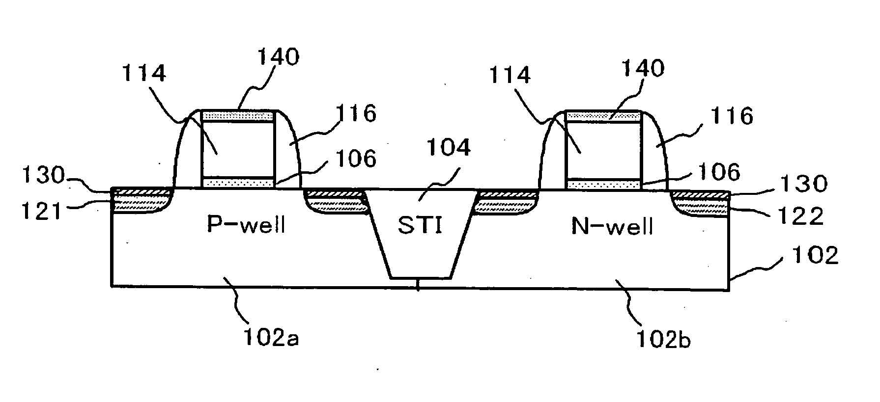
[0044]FIG. 1 is a cross-sectional view showing a configuration for a semiconductor device of this embodiment. In this embodiment, semiconductor device 100 is a CMOS (Complementary Metal Oxide Semiconductor) device containing an N-type MOSFET 118 and a P-type MOSFET 120. Further, this CMOS device constitutes the internal circuit of an LSI.
[0045] The semiconductor device 100 contains a silicon substrate 102 provided with a P-well 102a of a P-type conductor and an N-well 102b of an N-type conductor, and an element isolation region 104 for isolating the P-well 102a and the N-well 102b. The N-type MOSFET 118 and the P-type MOSFET 120 are formed at the P-well 102a and the N-well 102b, respectively. An inter-layer insulation film 134 covering the side of the N-type MOSFET 118 and the P-type MOSFET 120 is formed on the silicon substrate 102.
[0046] A pair of impurity diffusion layers 121 is provided at the P-well 102a, with a channel region being formed between these impurity diffusion lay...
second embodiment
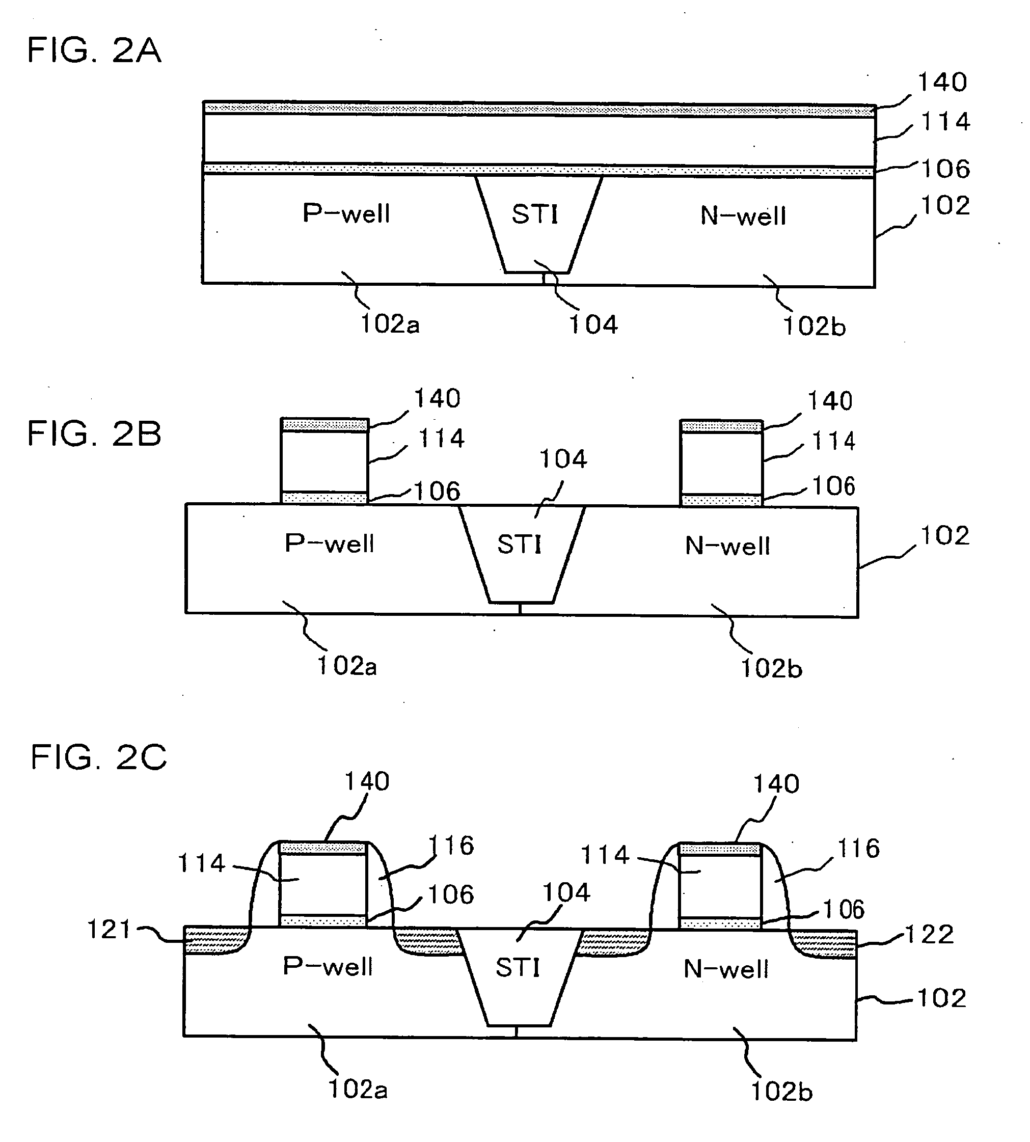
[0082] In this embodiment, part of the procedure for manufacturing the semiconductor device 100 is different to the first embodiment. The following is a description with reference to FIGS. 5A to 5C of a method for manufacturing a semiconductor device of this embodiment. FIGS. 5A to 5C are cross-sectional views of processes showing part of a procedure for manufacturing the semiconductor device 100 of this embodiment.
[0083] In this embodiment also, a structure that is the same as the structure shown in FIG. 3B is formed using the same procedure described with reference to FIGS. 2A to 2C, 3A and 3B in the first embodiment. The protective film 140 is selectively removed by, for example, dry etching, and the polysilicon film 114 is exposed (FIG. 5A).
[0084] Next, the second metal layer 144 (of a film thickness of, for example, 5 nm to 10 nm) is formed over the whole surface on the silicon substrate 102 (FIG. 5B). After this, second heat treatment is carried out. The metal composing the ...
third embodiment
[0087] In this embodiment, part of the procedure for manufacturing the semiconductor device 100 is different to the first embodiment. The following is a description with reference to FIGS. 6A to 6C, 7A, 7B and 8A to 8C of a method for manufacturing a semiconductor device of this embodiment. FIGS. 6A to 6C, 7A, 7B and 8A to 8C are cross-sectional views of processes showing part of a procedure for manufacturing the semiconductor device 100 of this embodiment.
[0088] First, as described in the first embodiment, the element isolation region 104, the P-well 102a, and the N-well 102b are formed on the silicon substrate 102, and the gate insulation film 106 and the polysilicon film 114 are formed on the silicon substrate 102 (FIG. 6A). This embodiment differs from the first embodiment in that a protective film 140 is not formed on the polysilicon film 114.
[0089] Next, selective etching is performed to form the gate shape in such a manner that predetermined regions of the gate insulation f...
PUM
 Abstract
Description
Claims
Application Information
 - R&D
- Intellectual Property
- Life Sciences
- Materials
- Tech Scout
- Unparalleled Data Quality
- Higher Quality Content
- 60% Fewer Hallucinations
Browse by: Latest US Patents, China's latest patents, Technical Efficacy Thesaurus, Application Domain, Technology Topic, Popular Technical Reports.
© 2025 PatSnap. All rights reserved.Legal|Privacy policy|Modern Slavery Act Transparency Statement|Sitemap|About US| Contact US: help@patsnap.com