Method of processing silicon wafer

a technology of silicon wafers and processing methods, applied in the direction of decorative surface effects, electrical appliances, decorative arts, etc., can solve the problems of degrading the surface of adjacent wafers, and achieve the effect of reducing the risk of contamination of adjacent wafers and simplifying the processing of the wafers

Active Publication Date: 2006-11-09
SUMCO CORP
View PDF2 Cites 20 Cited by
  • Summary
  • Abstract
  • Description
  • Claims
  • Application Information

AI Technical Summary

Benefits of technology

[0020] As described above, the inventive method relates to an improved method for processing a silicon wafer, the method comprising a slicing step in which a single crystal ingot is sliced into thin disc-like wafers, a lapping step in which the surface of each wafer is lapped to be planar, an alkaline cleaning step in which the wafer is subjected to alkaline cleaning to be removed of contaminants resulting from preceding machining, and an etching step in which the wafer is alternately transferred between two groups of etching tanks one of which contain acidic etching solutions and the other alkaline etching solutions. The feature of the inventive method lies in its including a beveling step between the slicing step and the lapping step in which a wafer is immersed in an acidic solution containing hydrofluoric acid (HF) and nitric acid (HNO3) at a volume ratio of ⅛ to ½ (HF / HNO3) so that degraded superficial layers occurring on the front and rear surfaces of the wafer as a result of machining can be removed and its edge surface can be beveled.
[0021] According to the inventive method described above, instead of mechanical beveling employed by the conventional method, a step is introduced in which a wafer is immersed in an acidic solution containing hydrofluoric acid (HF) and nitric acid (HNO3) at a volume ratio of ⅛ to ½ (HF / HNO3) which enables simultaneously the removal of degraded superficial layers resulting from preceding machining as well as beveling of the edge of the wafer. Thus, the method simplifies processing of the wafer. The method further dispenses with the necessity of alkaline cleaning which must be introduced subsequent to mechanical machining, which will reduce the risk of the wafer being contaminated with metal impurities, particularly Cu-based impurities associated with alkaline cleaning.

Problems solved by technology

The peripheral edge of a wafer is beveled because a wafer whose peripheral edge is not beveled and thus is rectangular will tend to develop notches and flaws, and silicon particles as a result of mechanical impacts to the wafer encountered by accident during transportation might degrade the surface of adjacent wafers.

Method used


Image

  • Method of processing silicon wafer
  • Method of processing silicon wafer
  • Method of processing silicon wafer

Examples


Embodiment Construction

[0022] The embodiments of the invention will be described below with reference to attached drawings.

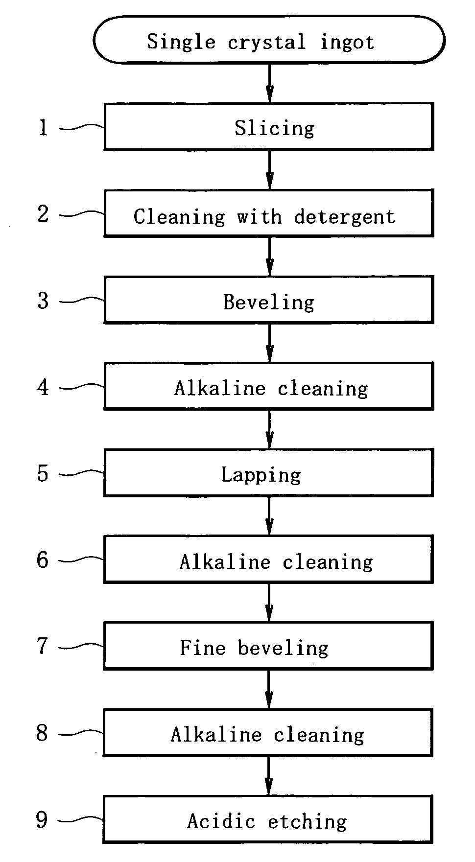
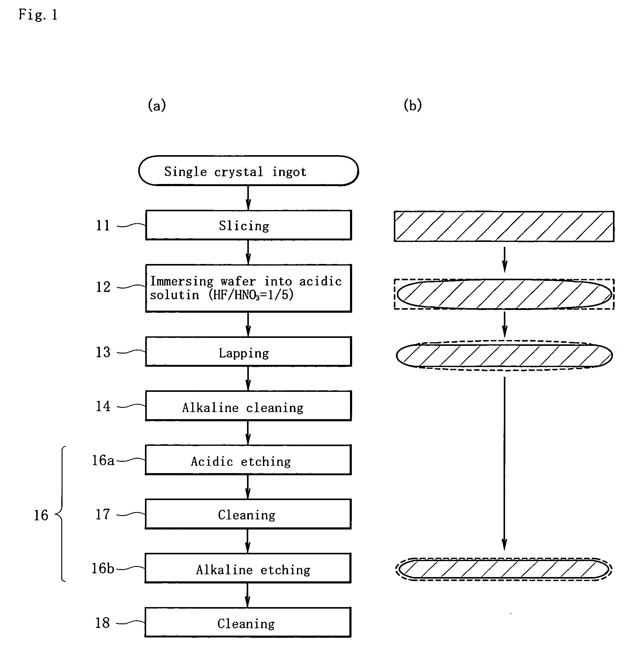
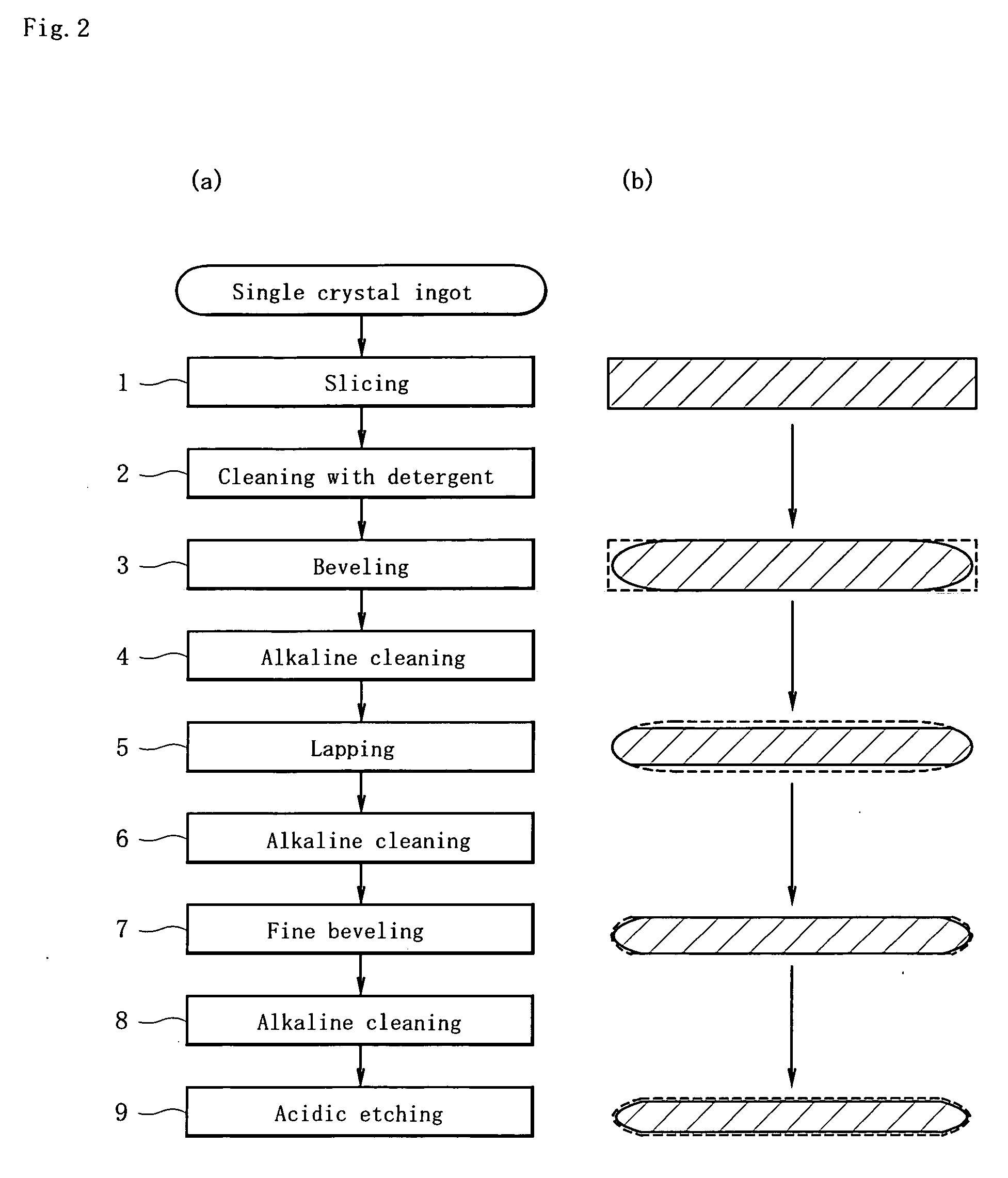
[0023] First, a grown single silicon crystal rod is cut at its frond and rear ends, and then divided into a number of blocks. The block has its periphery abraded until it becomes a cylinder having a uniform diameter. Then, an orientation flat or a notch is formed to mark the specified orientation of the crystal to produce a single crystal ingot product. The orientation flat and the notch are utilized as a reference for placing the wafer properly with respect to masks in a subsequent step during its elaboration into a device. After the step, the single crystal ingot is sliced at a specified angle to the longitudinal axis of the ingot with the blade of a cutter into thin, disc-like slices, thereby producing a plurality of silicon wafers as shown in FIG. 1(a) (step 11). FIG. 1(b) shows the cross-sections of silicon wafers having undergone the corresponding steps of FIG. 1(a).

[0024] Acc...


PUM

PropertyMeasurementUnit
thicknessaaaaaaaaaa
thicknessaaaaaaaaaa
volume ratioaaaaaaaaaa

Abstract

The inventive method for processing a silicon wafer is a method comprising step 11 in which a single crystal ingot is sliced into thin disc-like wafers; step 13 in which the surface of each wafer is lapped to be planar; step 14 in which the wafer is subjected to alkaline cleaning to be removed of contaminants resulting from preceding machining; and step 16 in which the wafer is alternately transferred between two groups of etching tanks one of which contain acidic etching solutions and the other alkaline etching solutions, wherein an additional step 12 is introduced between step 11 and step 13 in which a wafer is immersed in an acidic solution containing hydrofluoric acid (HF) and nitric acid (HNO3) at a volume ratio of ⅛ to ½ (HF/HNO3) so that degraded superficial layers occurring on the front and rear surfaces of the wafer as a result of machining can be removed and the edge surface of the wafer can be beveled. The inventive method simplifies the steps involved in the processing of a wafer, and reduces the intervention of alkaline cleaning accompanied with mechanical beveling, thereby reducing the risk of contamination due to metal impurities which may result from alkaline cleaning.

Description

CROSS-REFERENCES TO RELATED APPLICATIONS [0001] This application claims International Application PCT / JP2004 / 007251 filed May 24, 2004 and priority of Japanese Application No. 2003-150261 filed May 28, 2003, the entire disclosure of which is hereby incorporated by reference. TECHNICAL FIELD [0002] The present invention relates to a method for processing a silicon wafer which can prevent contamination due to metal impurities which would otherwise occur as a result of the cleaning of the wafer performed subsequent to its having undergone various machining processes. BACKGROUND ART [0003] Following steps have been disclosed as a conventional method for the processing of a silicon wafer (see, for example, Nonpatent literature 1). [0004] A single silicon crystal rod pulled up from a crucible is cut at its frond and rear ends, and then divided into a number of blocks. The block has its periphery abraded until it has a diameter close to a desired one. Then, an orientation flat or a notch i...

Claims


Application Information

Patent Timeline
Patent Type & Authority Applications(United States)
IPC IPC(8): H01L21/302H01L21/461H01L21/304H01L21/306
CPCH01L21/02008H01L21/30604H01L21/02052H01L21/02021H01L21/304
Inventor KOYATA, SAKAETAKAISHI, KAZUSHIGE
Owner SUMCO CORP
Why Eureka
Try Eureka