Wiring board and method of manufacturing the same

a technology of wiring board and etching process, which is applied in the direction of conductive pattern reinforcement, high current circuit adaptation, instruments, etc., can solve the problems of increasing the proportional time required for etching processing for processing circuit pattern layers, limiting the filler content, and reducing the thermal resistance. , the effect of excellent heat dissipation

Active Publication Date: 2006-11-16
FUJI ELECTRIC HLDG CO LTD
View PDF17 Cites 48 Cited by
  • Summary
  • Abstract
  • Description
  • Claims
  • Application Information

AI Technical Summary

Benefits of technology

[0020] Since in the wiring board according to the present invention the circuit pattern of the foil can be formed at least partially thicker, when a power semiconductor is mounted on this thick circuit pattern, the heat that is generated by losses therein can be diffused by the thick

Problems solved by technology

However, in the case of epoxy resin containing inorganic filler such as SiO2, Al2O3 or AlN, there are limits to the filler content, so the thermal conduction coefficient of such material is currently about 7 to 10 W/m·K.
There are therefore also limits to the current capacity of the power semiconductor modules in which these can be employed; currently they can only be employed in modules up to about the 50 A class.
However, in the case of metal base wiring boards, the thermal resistance is reduced, so, if thick copper foil is employed, the time required for the etching processing for processing the circuit pattern layer is increased in proportion to the thickness; processing costs are thereby greatly increased, giving rise to the problem that overall costs are greatly increased.
Furthermore, if the thickness of the circuit pattern layer reaches 3 to 4 mm, a long time is required for melting of the copper and, in a

Method used


Image

  • Wiring board and method of manufacturing the same
  • Wiring board and method of manufacturing the same
  • Wiring board and method of manufacturing the same

Examples


Embodiment Construction

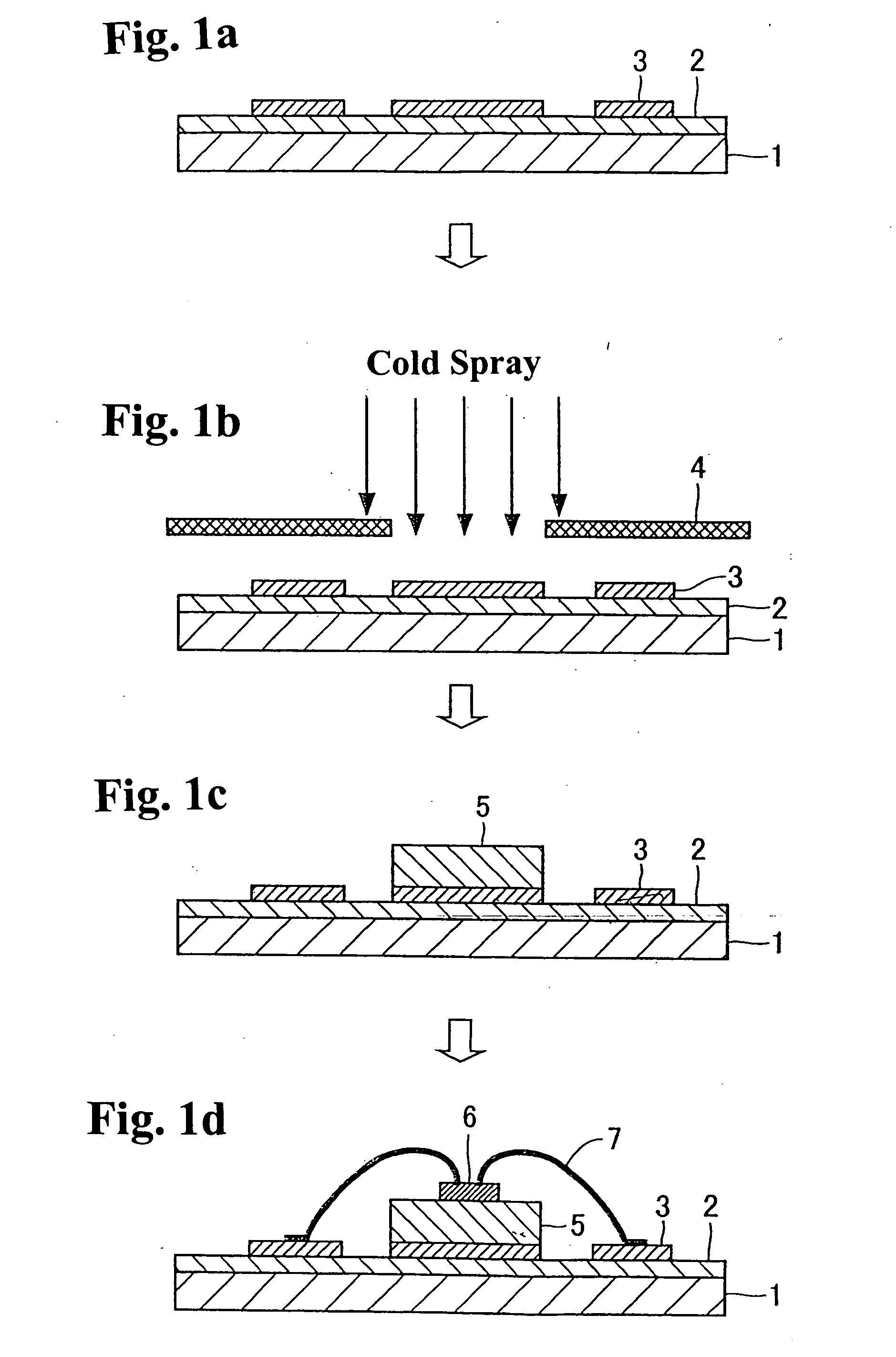
[0025] Hereinbelow, an embodiment of the present invention is described in detail with reference to the drawings in which the invention is applied to an example wherein a metal foil is attached to an insulating layer and a metal base printed wiring board is formed with a prescribed circuit pattern by processing this metal foil.

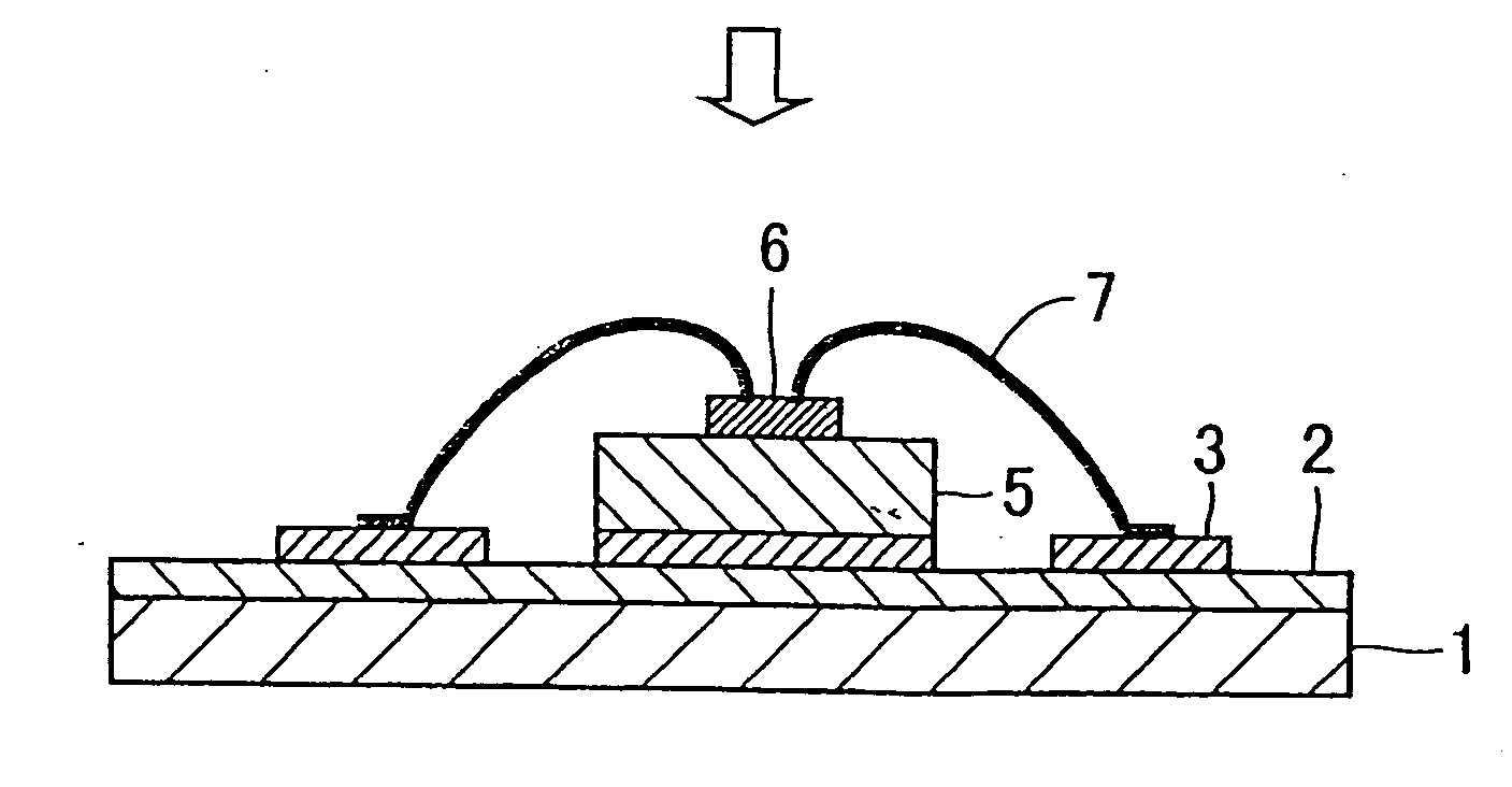
[0026]FIGS. 1a-1d show the process of manufacturing a wiring board according to the present invention and the condition of a completed power semiconductor module, wherein FIG. 1a shows a metal base wiring board, FIG. 1b shows the step of forming a built-up circuit pattern using a cold spray process, FIG. 1c shows a condition in which a built-up circuit pattern has been formed, and FIG. 1d shows a power semiconductor module in which a power semiconductor is mounted on a built-up circuit pattern.

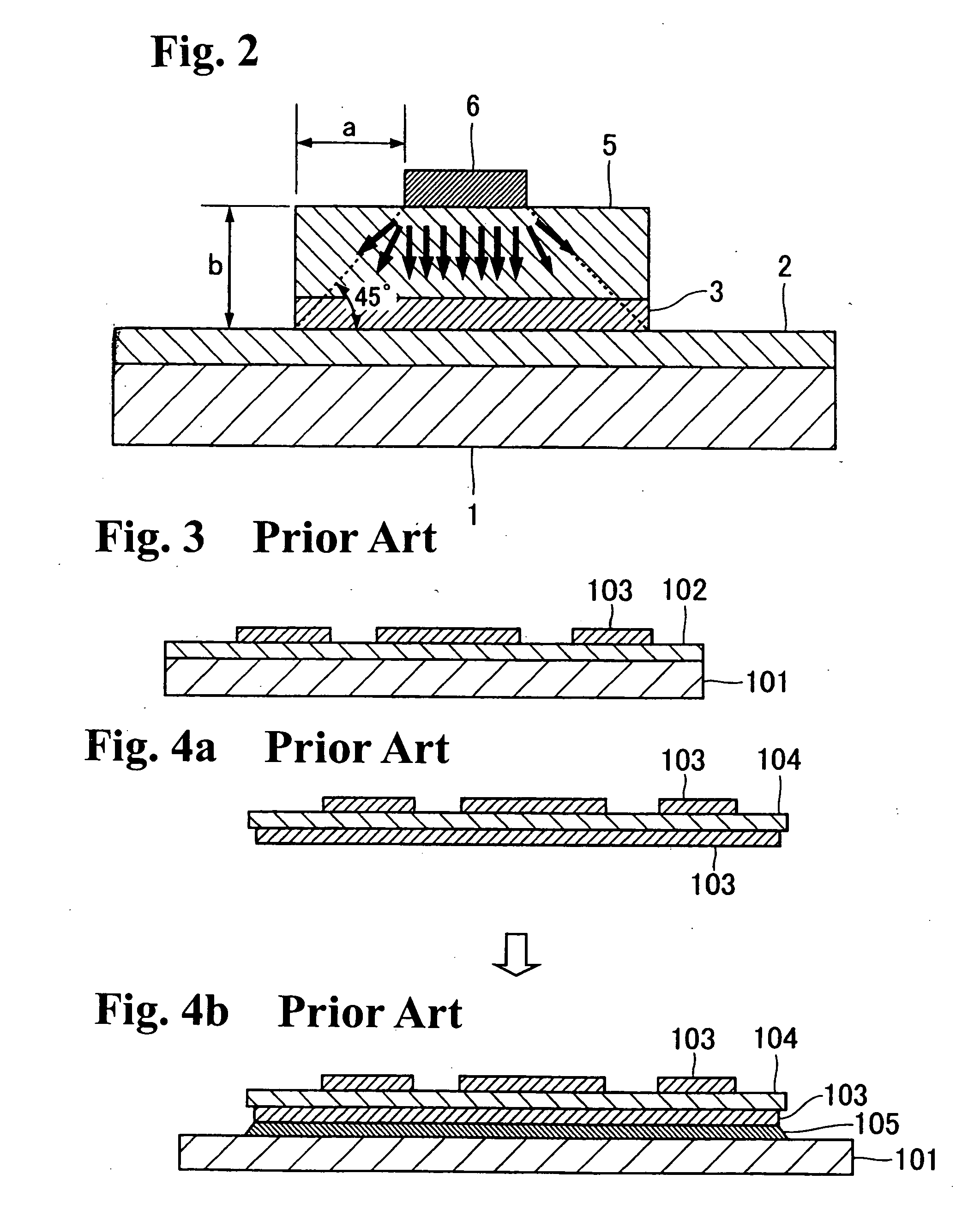
[0027] As shown in FIG. 1a, a metal base wiring board is of a three-layer construction constituted by providing an insulating layer 2 containing inorganic filler on ba...


PUM

PropertyMeasurementUnit
Thicknessaaaaaaaaaa
Deformation enthalpyaaaaaaaaaa
Dissipation factoraaaaaaaaaa

Abstract

A wiring board has a circuit pattern that includes metal foil attached to an insulating layer, and a built-up circuit pattern disposed on top of the metal foil circuit pattern. The built-up circuit pattern is an increased thickness laminate of cold spray processed metal material. Even when a power semiconductor is mounted on the built-up circuit pattern, the heat that is generated by losses therein can be diffused by the built-up circuit pattern. The wiring board has excellent heat dissipation, can be manufactured by a small number of process steps, and is of low cost.

Description

BACKGROUND OF THE INVENTION AND RELATED ART STATEMENT [0001] The present invention relates to a wiring board and a method of manufacturing the same. In particular, the invention relates to a wiring board of excellent heat dissipating properties which is capable of being applied to power source equipment for industrial use, and a method of manufacturing the same. [0002] Semiconductor modules employed in power source devices are applied over a wide range, from domestic equipment such as domestic air-conditioners or refrigerators, to industrial equipment such as inverters or servo controllers. In particular, a metal base wiring board or ceramic wiring board, which has excellent heat dissipating properties, is employed in for example IGBT (Insulated Gate Bipolar Transistor) modules incorporating power semiconductors, on account of the large amount of heat which these generate. [0003]FIG. 3 is a view showing the cross-sectional construction of a conventional metal base wiring board. [000...

Claims


Application Information

Patent Timeline
IPC IPC(8): H01L21/00G01R31/02
CPCH01L23/3735H01L2924/1305H05K1/0203H05K1/0263H05K1/0306H05K1/056H05K3/24H05K2203/1344H01L2224/48091H01L2924/3011Y10T29/49155Y10T29/4913H01L2924/13055H01L2224/45124H01L2924/00014H01L2924/00
Inventor OKAMOTO, KENJI
Owner FUJI ELECTRIC HLDG CO LTD
Why Eureka
Try Eureka