[0004] At the
present day, the voltage controlled oscillator is mainly applied to a cellular phone
wireless transceiver of a communication
system such as
GSM (
Global System for Mobile communications), PDC (Personal Digital Cellular), PHS (Personal Handy-phone
System), or PCS (Personal Communication Services), or a
wireless transceiver that a
wireless LAN (
Local Area Network) that conforms to 802.11a, 802.11b, and 802.11g which is the wireless communication specifications defined by the IEEE standard. Also, there are various frequencies that are used in the above communication
system and wireless communication specifications. Lower prices, smaller sizes, and lower
power consumption for long-time operations are always in demand for those wireless transceivers. As one of the methods of meeting those needs, there is a method in which the wireless communication circuit is realized by a smaller number of
semiconductor integrated circuits (hereinafter referred to as “IC”). In particular, attempts have been frequently conducted to realize the wireless communication circuit by a
silicon (Si) IC because the substrate material is low in cost, and the high yield is ensured by the high maturity of a
semiconductor process. Up to now, there have been proposed a large number of wireless transceivers that are low in price and small in size. In future developments, lower prices and smaller sizes will be demanded, and it is expected to realize a
wireless transceiver that is capable of conforming to the above plural wireless communication specifications in order to conduct an optimum wireless communication according to the whereabouts of a user or a user's purpose.
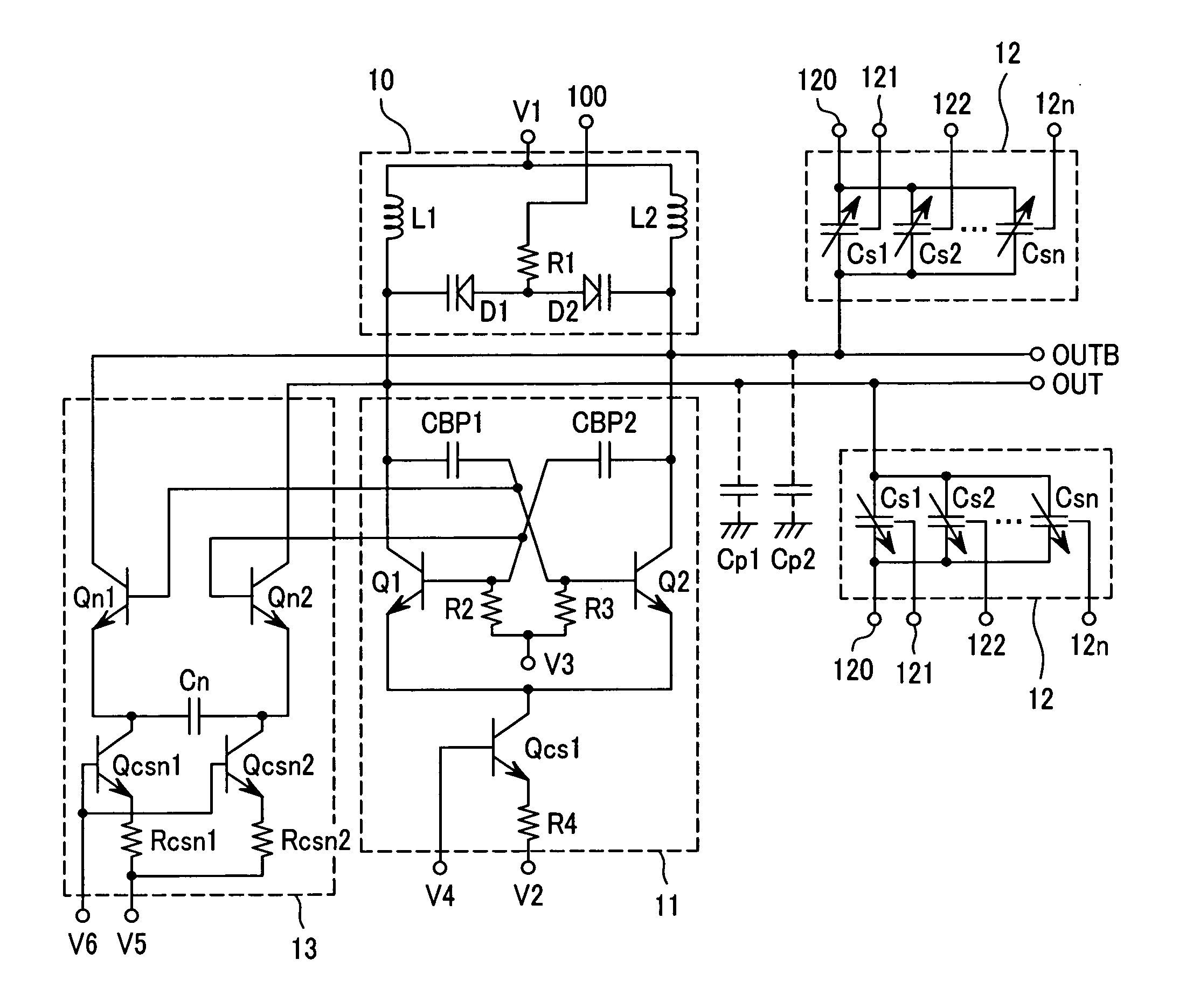
[0009] A positive phase terminal (+) and a
negative phase terminal (−) that are differential terminals of the
LC resonant circuit 10 are connected to a positive phase terminal (+) and a
negative phase terminal (−) of the
negative conductance generator circuit 11, to thereby form a positive phase resonation node OUT and a
negative phase resonation node OUTB. The
negative conductance generator circuit 11 is used for the purposes of generating a negative conductance to supplement the loss of electric powers that are generated in the resonation nodes OUT and OUTB, and to maintain the oscillation as an oscillator. A different signal is outputted from the resonation nodes OUT and OUTB.
[0020] In order to achieve the above object, a typical example of the present invention will be described below. That is, according to the present invention, there is provided a voltage controlled oscillator comprises a differential negative conductance generator circuit having first and second terminals for differential output, a differential resonant circuit having a variable capacitance which is controlled by
voltage control and an
inductance connected in parallel to each other, wherein the differential resonant circuit is connected between the first terminal and the second terminal, and a differential negative impedance circuit connected between the first terminal and the second terminal, wherein a capacitance of a capacitor with a constant capacitance that occurs between the first terminal and the second terminal is reduced by a negative impedance of the negative impedance circuit. In this way, because the capacitance of the capacitor with the constant capacitance is reduced, it is possible to increase a variable amount of the capacitance of the
resonant capacitor in the resonant circuit. This makes it possible to expand a variable range of the oscillation frequency of the voltage controlled oscillator. The capacitor with the constant capacitance is represented by floating capacitors that occur between the first terminal and a voltage with ground potential and between the second terminal and the voltage with ground potential, respectively.
[0021] It is desirable to connect, between the first terminal and the second terminal, a differential capacitor
bank having at least one pair of capacitors which is connected in parallel, each pair of the at least one pair of capacitors having two capacitors connected in series and a capacitance of each capacitor of the at least one pair of capacitors changing to two values according to high and low of a magnitude of a supply voltage. Alternatively, it is desirable to connect, between the first terminal and the ground potential and between the second terminal and the ground potential, capacitor banks having at least one capacitor that is connected in parallel, each capacitor of the at least one capacitor changing to two values according to high and low of the magnitude of a supply voltage, respectively. This makes it possible to expand further a variable range of the oscillation frequency of the voltage controlled oscillator.
[0023] According to the present invention, because the negative impedance circuit is disposed in the voltage controlled oscillator to reduce the capacitance of the capacitor with the constant capacitance, the variable amount of the capacitance of the resonant capacitor in the resonant circuit can be increased, thereby making it possible to expand the variable range of the oscillation frequency of the voltage controlled oscillator.

