

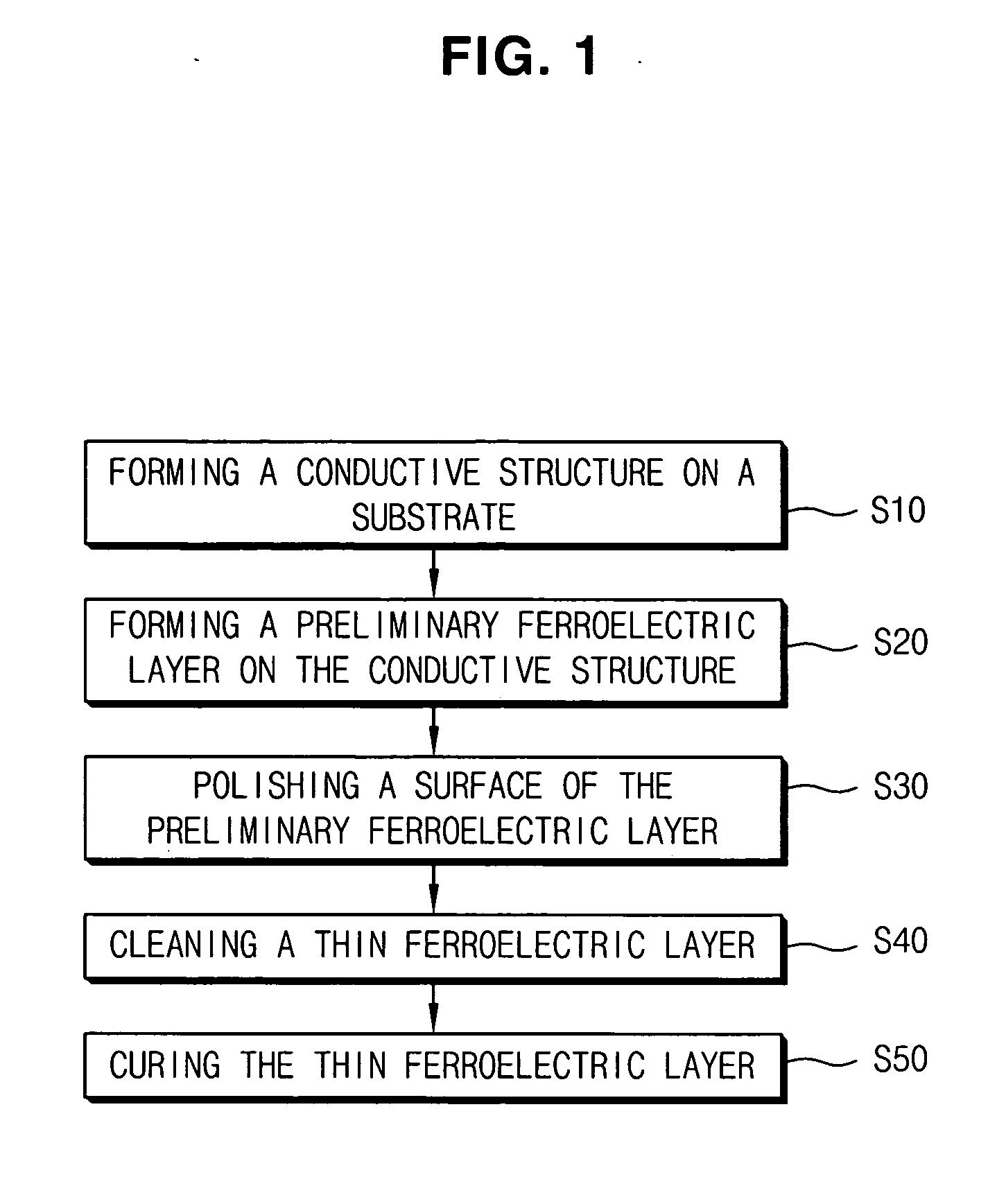
Methods of fabricating thin ferroelectric layers and capacitors having ferroelectric dielectric layers therein
a technology of ferroelectric dielectric layer and ferroelectric layer, which is applied in the direction of manufacturing tools, lapping machines, instruments, etc., can solve the problems of poor fatigue characteristics of the ferroelectric layer of pzt, poor electrical and ferroelectric characteristics of the framing device including the rough ferroelectric layer, and poor fatigue characteristics of the framing device, so as to improve the ferroelectric and electrical characteristics, enhance polarization or data retention, and uniform thin thickness
- Summary
- Abstract
- Description
- Claims
- Application Information
AI Technical Summary
Benefits of technology
Problems solved by technology
Method used
Image

Examples
example 1
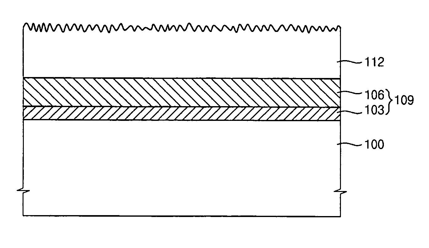
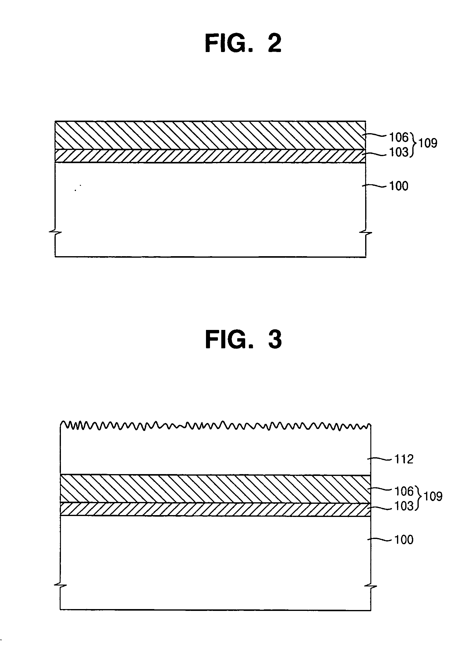
[0193] After a first conductive layer and a second conductive layer were sequentially formed on a substrate, a preliminary ferroelectric layer was formed on the second conductive layer. The first and the second conductive layers were formed using titanium aluminum nitride and iridium, respectively. The preliminary ferroelectric layer was formed using PZT by an MOCVD process. The first conductive layer had an average thickness of about 300 Å, and the second conductive layer had an average thickness of about 1,200 Å. The preliminary ferroelectric layer had an average thickness of about 1,000 Å.
[0194] A surface of the preliminary ferroelectric layer was polished using a slurry by a CMP process to thereby form a thin ferroelectric layer. The slurry included an abrasive that contains acidic silica having a pH of about 2.5. The preliminary ferroelectric layer was polished for about 30 seconds. In the CMP process, a downward pressure was about 8.5 psi, and a rotation speed of a polishing ...
example 2
[0195] After a first conductive layer and a second conductive layer were sequentially formed on a substrate, a preliminary ferroelectric layer was formed on the second conductive layer. The first and the second conductive layers were formed using titanium aluminum nitride and iridium, respectively. The preliminary ferroelectric layer was formed using PZT by an MOCVD process. The first conductive layer had an average thickness of about 300 Å, and the second conductive layer had an average thickness of about 1,200 Å. The preliminary ferroelectric layer had an average thickness of about 1,000 Å.
[0196] A surface of the preliminary ferroelectric layer was polished using a slurry by a CMP process so that a thin ferroelectric layer was formed on the second conductive layer. The slurry included an abrasive that contains acidic silica having a pH of about 2.1. The preliminary ferroelectric layer was polished for about 60 seconds. In the CMP process, a downward pressure was about 8.5 psi, an...
example 3
[0202] After a first conductive layer and a second conductive layer were sequentially formed on a substrate, a preliminary ferroelectric layer was formed on the second conductive layer. The first and the second conductive layers were formed using titanium aluminum nitride and iridium, respectively. The preliminary ferroelectric layer was formed using PZT by an MOCVD process. The first and the second conductive layers had average thicknesses substantially identical to those of the first and the second conductive layers in Example 1. The preliminary ferroelectric layer had an average thickness of about 1,100 Å.
[0203] A surface of the preliminary ferroelectric layer was polished using a slurry by a CMP process to thereby form a thin ferroelectric layer on the second conductive layer. The slurry included an abrasive that contains acidic silica having a pH of about 2.1. The preliminary ferroelectric layer was polished for about 15 seconds. In the CMP process, a downward pressure was abo...
PUM
 Abstract
Description
Claims
Application Information