This helps you quickly interpret patents by identifying the three key elements:
Problems solved by technology
Method used
Benefits of technology
Benefits of technology
[0016] The present invention is provided in view of the above-described problem, and an object thereof is to provide a wire structure having excellent electromigration resistance and stress migration resistance, as well as a method for forming the same.
[0019] According to the wire structure and a method for forming the same of the present invention, an interlayer diffusion preventing film made of a high melt point metal or a high melt point metal compound is formed on top of a lower layer wire, and a via hole and an upper layer trench are formed in a second insulating layer as an upper layer, and after that, the interlayer diffusion preventing film is etched so that the material thereof adheres to the side walls (sides of the second insulating film) at the bottom of the via hole. As a result, even in the case where the lower layer wire (for example, a copper wire) is etched through this etching, the metal material of the lower layer wire does not adhere to the side walls at the bottom of the via hole. That is to say, though in general, the width of via holes is no greater than the width of lower layer wires and the side walls at the bottom of via holes are close to the upper surface of lower layer wires, and therefore, the metal material of lower layer wires easily adheres to second insulating films at the time of etching, an adhering film can prevent the metal material from adhering to the second insulating film without fail according to the present invention. As a result of this, the metal material of the first wire does not diffuse into the second insulating layer, and thus, the electromigration resistance increases.
[0020] Further, a second diffusion preventing film that is formed in post processing is formed on the sides of the second insulating layer with the adhering film as a base so as to have a film thickness of no less than 5 nm, which is thicker than that of the conventional art 1. Therefore, the material (for example, copper) of the conductor that is formed within the via hole can be effectively prevented from diffusing into the second insulating layer, and at the same time, the electromigration resistance increases.
[0021] In addition, according to the present invention, a diffusion preventing film made of a high melt point metal or a high melt point metal compound is formed on the upper surface of the first wire, and therefore, the film stress in the interface between the first wire and the interlayer diffusion preventing film is stable, and as a result, the stress migration resistance increases, and a highly reliable wire structure can be gained.
Problems solved by technology
It is difficult to process copper in accordance with a conventional dry etching method, and it is necessary to form wires in accordance with a Damascene method, where a trench for copper wire is formed in advance in an insulating layer, a metal film is formed on the entire surface in such a manner that this trench is filled with the metal film, and the metal film on the insulating layer is removed in accordance with a chemical mechanical polishing method (CMP method) in such a manner that the metal film remains only in the trench.
As a result of this, there is a possibility that copper may diffuse into the second insulating film 908, and electromigration resistance and stress migration resistance may be deteriorated.
Method used
Image
Click on the blue label to locate the original text in one second.
Reading with bidirectional positioning of images and text.
Examples
first embodiment
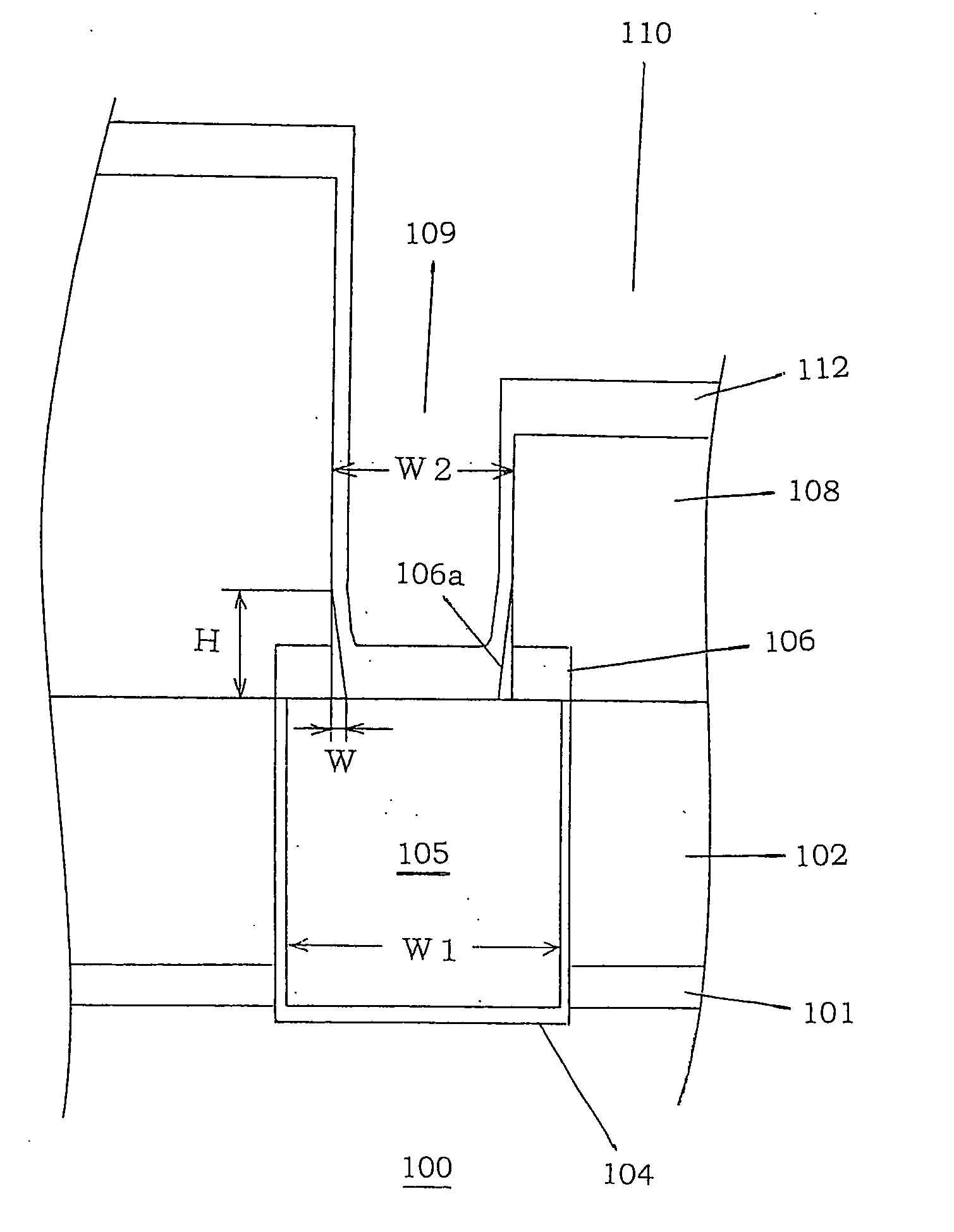
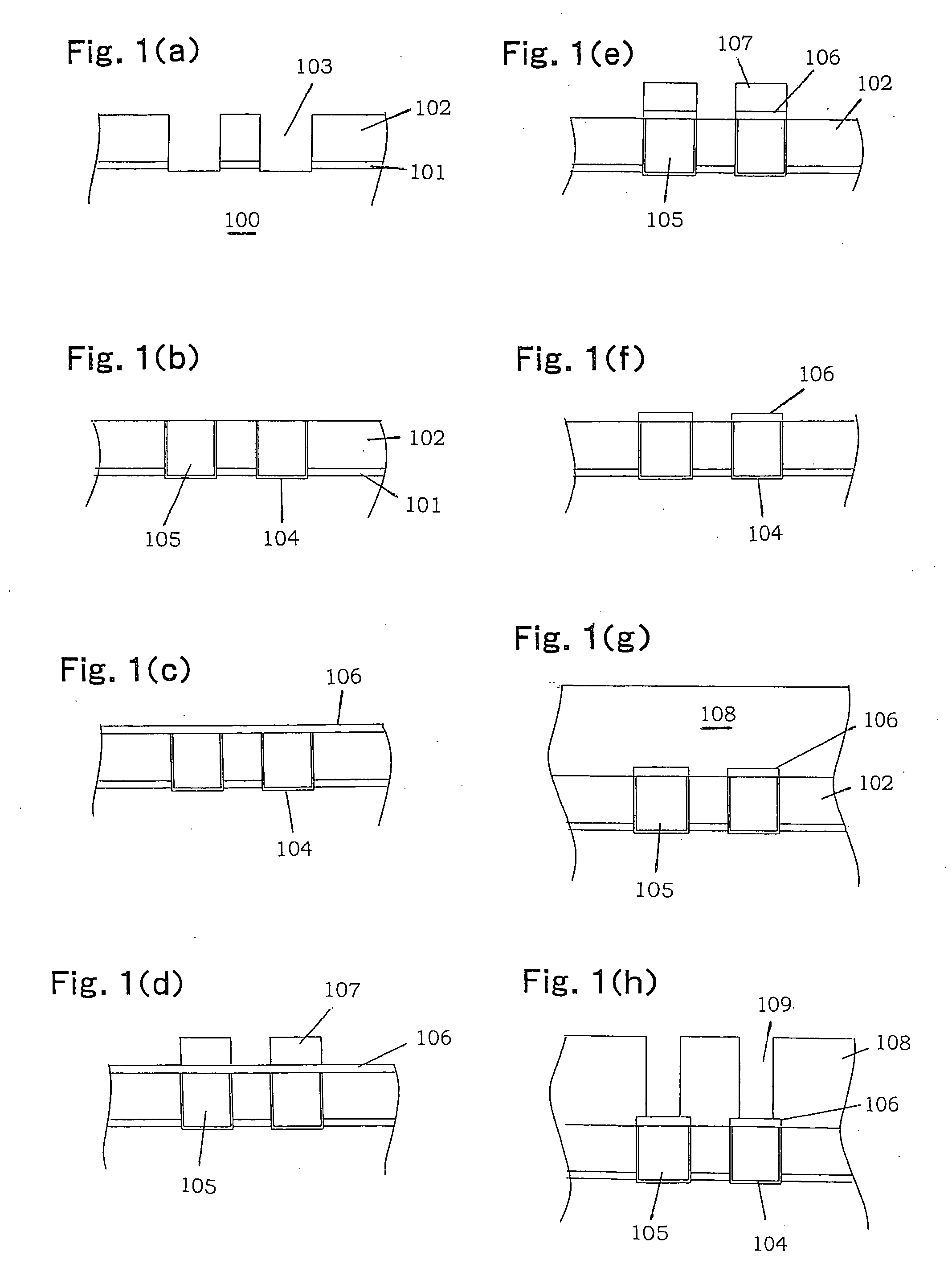
[0050]FIGS. 1 and 2 respectively show cross sectional diagrams each illustrating a portion of the wire structure during the manufacturing process according to a first embodiment of the present invention.
[0051] The forming method for a wire structure according to this first embodiment is concretely described in the following. First, an etching stopping film 101 made of Si3N4 is formed on top of a semiconductor substrate 100, and furthermore, a first insulating layer 102 is formed so as to have a film thickness of 200 nm to 400 nm. The first insulating layer 102 is dry etched using a photoresist film (not shown) as a mask so that a plurality of first trenches (lower layer trenches) 103 are formed (see FIG. 1(a)).
[0052] Next, a first diffusion preventing film 104 made of TaN is formed so as to cover the surface of the first insulating layer 102 and the inner surface of the respective first trenches 103, and have a film thickness of 10 nm to 20 nm. A copper seed film is formed on the ...
second embodiment
[0065]FIGS. 4 and 5 respectively show cross sectional diagrams each illustrating a portion of the wire structure during the manufacturing process according to a second embodiment of the present invention. Here, mainly points of the second embodiment which are different from the first embodiment are described in detail.
[0066] In the second embodiment, as shown in FIG. 4(a), a copper film 205a having a film thickness of 100 nm to 150 nm is formed on a first insulating layer 202 with a first diffusion preventing film (TaN) 204 having a film thickness of 10 nm to 20 nm in between, in accordance with the same method as that in the first embodiment, so as to completely fill in the first trenches. Next, as shown in FIG. 4(b), the copper film 205a and the first diffusion preventing film 204 on the first insulating layer 202 are removed in accordance with a CMP method where the polishing rate of the metal film is higher than that of the first insulating layer 202, so that first wires 205 ar...
third embodiment
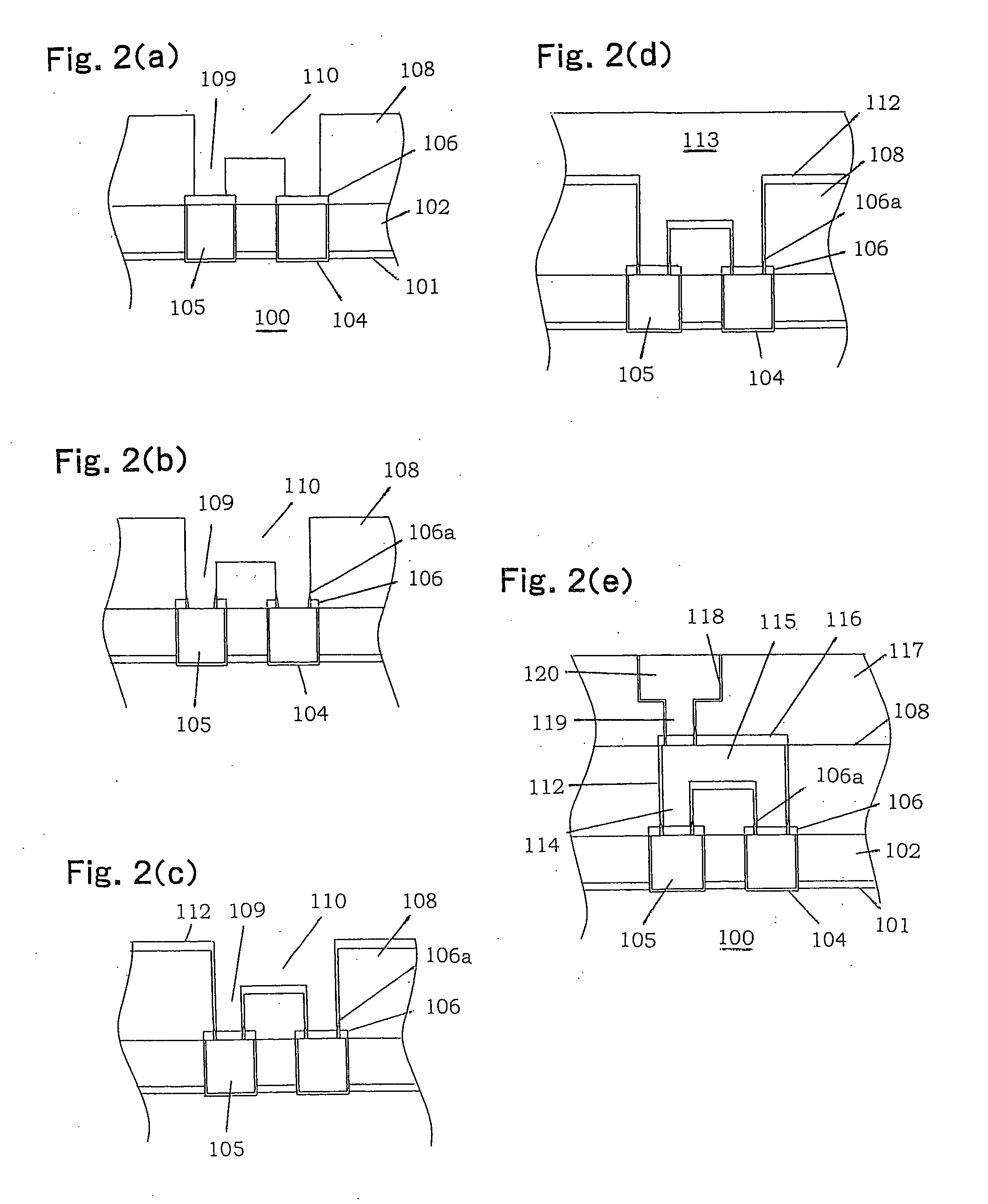
[0073]FIGS. 6 and 7 respectively show cross sectional diagrams each illustrating a portion of the wire structure during the manufacturing process according to a third embodiment of the present invention.
[0074] In this third embodiment, the second and third layers, which are insulating layers, are formed so as to have a single Damascene wire structure. First, as shown in FIGS. 6(a) to 6(c), a first interlayer diffusion preventing film 306 made of TaN having a film thickness of approximately 10 nm to 50 nm is formed on a first wires 305 and a first insulating layer 302 in accordance with a sputtering method, which is the same method as in the first embodiment. The first interlayer diffusion preventing film 306 on the first insulating layer 302 is removed through etching using a resistmask 307 while leaving the first interlayer diffusion preventing film 306 on the first wires 305, and after that, the resistmask 307 is removed. Here, in FIG. 6(a), a numeric symbol 300 indicates a sem...
PUM
Abstract
A wire structure, comprising: a first insulating layer having a lower layer trench formed in an outer surface thereof; a first diffusion preventing film formed on an inner surface of the lower layer trench; a lower layer wire filled in the lower layer trench through the first diffusion preventing film; an interlayer diffusion preventing film formed on the lower layer wire, the interlayer diffusion preventing film made of a high melt point metal or a high melt point metal compound; a second insulating layer formed over the first insulating layer and the interlayer diffusion preventing film, a second insulating layer having a via hole that penetrates through the second insulating layer and the interlayer diffusion preventing film so as to reach the lower layer wire; a conductive second diffusion preventing film formed on an inner surface of the via hall; a conductor filled in the via hole through the second diffusion preventing film, and an adhering film made of the material that forms the interlayer diffusion preventing film, wherein the adhering film is formed so as to extend from an upper surface of the lower layer wire to a side surface of the second insulating layer within the via hall.
Description
CROSS-REFERENCE TO RELATED APPLICATION [0001] This application is related to Japanese Patent Application No. 2005-148110 filed on May 20, 2005, whose priory is claimed and the disclosure of which is incorporated by reference in its entirety. BACKGROUND OF THE INVENTION [0002] 1. Field of the Invention [0003] The present invention relates to a wire structure and a forming method of the same, and in particular, to a wire structure having a multilayer wire structure which is formed in accordance with a Damascene method using copper, where electromigration resistance and stress migration resistance is increased, as well as a forming method of such a wire structure. [0004] 2. Description of the Related Art [0005] Together with the miniaturization of semiconductor devices, wires have also become miniaturized, and as a result, wire resistance and capacitance between wires has increased, and a wire material having a lower resistance has come to be required, in order to increase the speed of...
Claims
Application Information
Patent Timeline
Application Date:The date an application was filed.
Publication Date:The date a patent or application was officially published.
First Publication Date:The earliest publication date of a patent with the same application number.
Issue Date:Publication date of the patent grant document.
PCT Entry Date:The Entry date of PCT National Phase.
Estimated Expiry Date:The statutory expiry date of a patent right according to the Patent Law, and it is the longest term of protection that the patent right can achieve without the termination of the patent right due to other reasons(Term extension factor has been taken into account ).
Invalid Date:Actual expiry date is based on effective date or publication date of legal transaction data of invalid patent.

