Semiconductor device

a technology of semiconductors and devices, applied in the direction of substantially flat resonant elements, resonant antennas, instruments, etc., can solve the problems of poor connection, low yield, disconnection or poor connection, etc., and achieve the effect of reducing the adverse effect of copper diffusion on the electrical characteristics of the circuit element, stress migration, and copper diffusion

Inactive Publication Date: 2010-07-06
SEMICON ENERGY LAB CO LTD
View PDF7 Cites 10 Cited by
  • Summary
  • Abstract
  • Description
  • Claims
  • Application Information

AI Technical Summary

Benefits of technology

[0011]It is an object of the present invention to prevent, in a semiconductor device having an integrated circuit and an antenna formed over the same substrate which uses copper plating for the antenna, electrical characteristics of a circuit element from being adversely affected by copper diffusion such as electromigration or stress migration. It is another object of the present invention to prevent a defect of a semiconductor device having an integrated circuit and an antenna formed over the same substrate, which is caused by poor connection between the antenna and the integrated circuit.
[0013]In a semiconductor device of the present invention having an integrated circuit and an antenna formed over one substrate, which uses copper plating for the antenna, a nitride film is used as a base layer of the antenna. Therefore, copper diffusion to a circuit element by electromigration, stress migration, or the like can be prevented and an adverse effect on electrical characteristics of the circuit element due to copper diffusion can be decreased. Moreover, the use of nickel nitride as metal nitride of the base layer of the antenna can improve the adhesion between the copper plating layer and the base layer of the antenna and can decrease poor connection between the antenna and the integrated circuit.

Problems solved by technology

In the case where an antenna and an integrated circuit are thus formed separately from each other and connected to each other, the both need to be electrically connected, which leads to low yield because of technical difficulty in connection between the antenna and a minute terminal of the integrated circuit.
Moreover, stress applied at a connection point in the use of a wireless chip causes disconnection or poor connection.
In particular, when a wireless chip is flexible, it is expected that poor connection is more likely to occur.
However, the present inventors found that the aforementioned conventional structure causes copper diffusion such as electromigration or stress migration, which adversely affects electrical characteristics of circuit elements in the integrated circuit formed over the same substrate as the antenna coil.

Method used


Image

  • Semiconductor device
  • Semiconductor device
  • Semiconductor device

Examples


embodiment mode 1

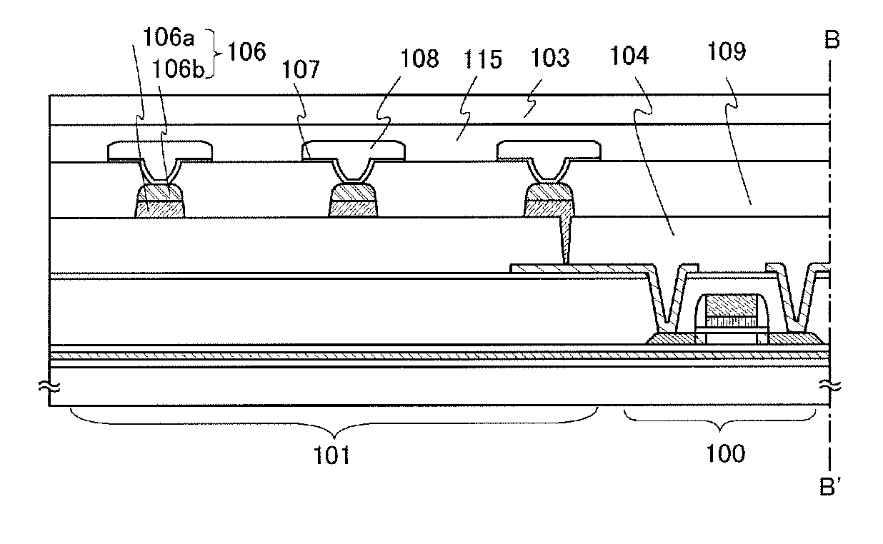
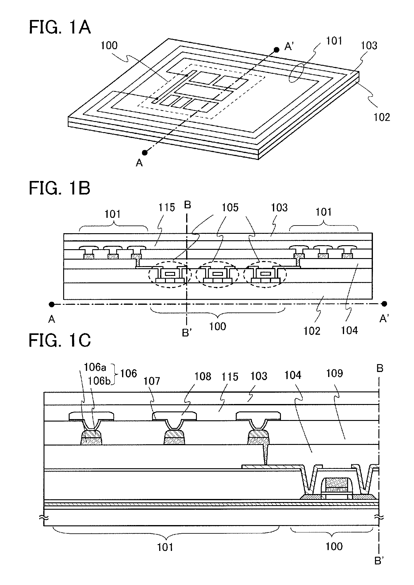
[0025]Embodiment Mode 1 of a semiconductor device of the present invention will hereinafter be described with reference to drawings. FIGS. 1A to 1C show a wireless chip as an example of a semiconductor device of the present invention. FIG. 1A is a perspective view of the wireless chip, FIG. 1B is a cross sectional view thereof along A-A′ of FIG. 1A, and FIG. 1C is a magnified view of a left part from a chain line B-B′ of FIG. 1B.

[0026]In FIG. 1A, an integrated circuit 100 and an antenna 101 are formed over one substrate 102 and covered by a cover member 103. A top surface of the antenna 101 has a rectangular and spiral shape, and the antenna 101 is electrically connected to the integrated circuit 100.

[0027]FIG. 1B is a cross sectional view along A-A′ of FIG. 1A. The integrated circuit 100 is formed over the substrate 102 and the antenna 101 is formed over a third interlayer insulating film 104 that covers the integrated circuit 100. A protection film 115 and the cover member 103 are...

embodiment mode 2

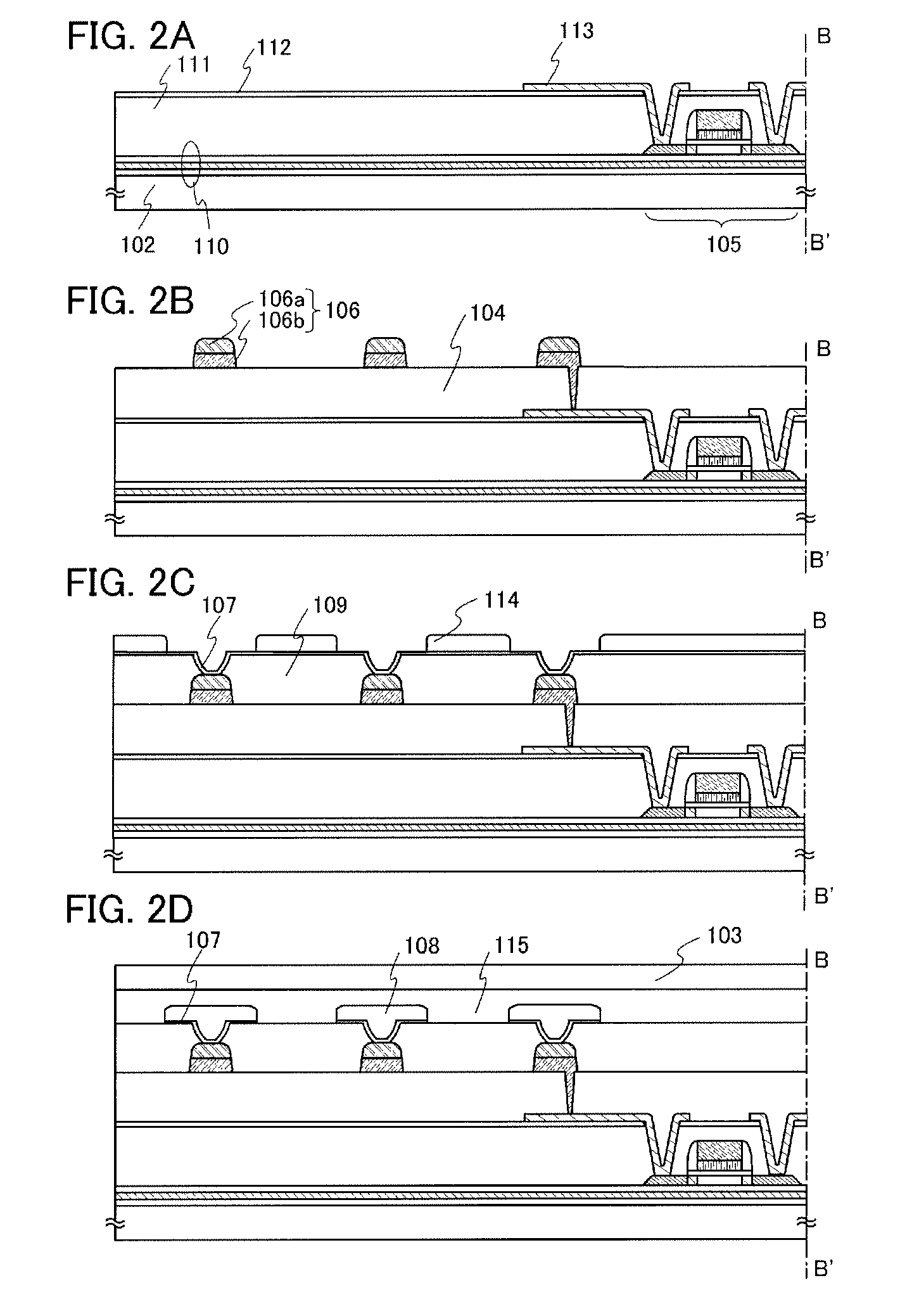
[0066]Another embodiment mode of a wireless chip as an example of a semiconductor device of the present invention will hereinafter be explained with reference to drawings. FIGS. 4A to 4C show a wireless chip as an example of a semiconductor device of the present invention. FIG. 4A is a perspective view of the wireless chip, FIG. 4B is a cross sectional view along A-A′ of FIG. 4A, and FIG. 4C is a magnified view of a left part from a chain line B-B′ of FIG. 4B.

[0067]Since FIGS. 4A and 4B are the same as FIGS. 1A and 1B in Embodiment Mode 1, the description is omitted.

[0068]FIG. 4C is the same as FIG. 1C except that the antenna base layer 107 of FIG. 1C in Embodiment Mode 1 is replaced by a first antenna base layer 107a and a second antenna base layer 107b. Therefore, description will hereinafter be made on only the first antenna base layer 107a and the second antenna base layer 107b.

[0069]The first antenna base layer 107a is formed over the lower wiring 106, and the second antenna b...

embodiment mode 3

[0080]Next, a method of manufacturing a wireless chip of another embodiment mode of the present invention will be explained in detail. Although this embodiment mode shows a TFT as an example of a semiconductor element used for an integrated circuit of a wireless chip, a semiconductor element used for an integrated circuit is not limited to this, and any kind of semiconductor element can be used.

[0081]First, a release layer 501 is formed over a first substrate 500 having heat resistance as shown in FIG. 5A. The first substrate 500 may be, for example, a glass substrate such as a barium borosilicate glass substrate or an aluminoborosilicate glass substrate, a quartz substrate, a ceramic substrate, or the like. Moreover, the first substrate 500 may be a semiconductor substrate or a metal substrate including a stainless steel substrate. A substrate formed of a synthetic resin having flexibility, such as plastic, generally tends to have lower allowable temperature limit than the above-de...


PUM


Abstract

An object of the present invention is to prevent electrical characteristics of circuit elements from being adversely affected by copper diffusion in a semiconductor device having an integrated circuit and an antenna formed over the same substrate, which uses copper plating for the antenna. Another object is to prevent a defect of a semiconductor device due to poor connection between an antenna and an integrated circuit in a semiconductor device having the integrated circuit and the antenna formed over the same substrate. In a semiconductor device having an integrated circuit 100 and an antenna 101 formed over one substrate 102, when a copper plating layer 108 is used for a conductor of the antenna 101, it is possible to prevent copper diffusion to circuit elements and decrease an adverse effect on electrical characteristics of circuit elements due to the copper diffusion because a base layer 107 of the antenna 101 uses a nitride film of a predetermined metal. Moreover, by the use of nickel nitride as a metal nitride for the base layer of the antenna, poor connection between the antenna and the integrated circuit can be decreased.

Description

BACKGROUND OF THE INVENTION[0001]1. Field of the Invention[0002]The present invention relates to a semiconductor device capable of input and output of information by using electromagnetic waves. It is to be noted that the semiconductor device in this specification refers to all devices that can function by utilizing semiconductor characteristics, and electro-optic devices, semiconductor circuits, and electrical appliances, which have this function, are all semiconductor devices.[0003]2. Description of the Related Art[0004]In recent years, wireless chips for RFID (radio frequency identification system) have been researched and put into practical use as an information and communication technology utilizing electromagnetic waves.[0005]RFID refers to a communication technology over electromagnetic waves between a reader / writer and a semiconductor device capable of wirelessly transmitting and receiving information (also called an RFID tag, an RF tag, an ID tag, an IC tag, a wireless tag,...

Claims


Application Information

Patent Timeline
Patent Type & Authority Patents(United States)
IPC IPC(8): H01Q1/38G06K19/02G06K19/07H01L21/768H01L21/822H01L23/532H01L27/04H01L29/423H01L29/49
CPCH01Q1/2208H01Q23/00H01Q9/0407
Inventor HANAOKA, KAZUYAOHNUMA, HIDETOFUJII, TERUYUKI
Owner SEMICON ENERGY LAB CO LTD
Why Eureka
Try Eureka