Multilayer multicomponent high-k films and methods for depositing the same

a technology of dielectric films and components, applied in the direction of chemical vapor deposition coatings, coatings, basic electric elements, etc., can solve the problems of capacitor structure formation, similar problems, and known devices no longer function, and achieve the effect of optimizing the performance of multi-layer structures

Inactive Publication Date: 2006-11-23
AVIZA TECHNOLOGY INC
View PDF42 Cites 425 Cited by
  • Summary
  • Abstract
  • Description
  • Claims
  • Application Information

AI Technical Summary

Benefits of technology

[0012] In another embodiment of the present invention, a multi-component film of a high-k material is provided comprising hafnium, titanium, silicon, oxygen, nitrogen, and combinations thereof. The high-k material may be used in the manufacture of semiconductor structures such as gates, capacitors, and the like.
[0013] In one embodiment of the present invention, the multi-component films are formed by providing suitable precursors containing the various components of the multi-component film. The precursors may be distinct chemical entities or may be appropriate mixtures of two or more components. The precursors may be introduced either simultaneously or sequentially during deposition. In an exemplary embodiment, precursors containing hafnium, titanium, and silicon are used.
[0014] In a further embodiment of the present invention, the multi-component films are formed by providing suitable reactant gases containing the various components of the multi-component films. The reactant gases comprise various chemical species that can be used to oxidize, nitride, or reduce the deposited layer. The reactant gases may be introduced either simultaneously or sequentially during the deposition.
[0015] In another embodiment of the present invention, multi-layer, multi-component film stacks forming a high-k gate film stack ar

Problems solved by technology

Under these conditions, known devices will no longer function.
Similar issues are faced in the formation of capacitor structures in semiconductor devices.
These materials have been found to be unsatisfactory for several reasons.
These metal oxides materials are not stable under subsequent processing conditions when deposited on silicon or silicon dioxide.
They react with underlying materials an

Method used


Image

  • Multilayer multicomponent high-k films and methods for depositing the same
  • Multilayer multicomponent high-k films and methods for depositing the same
  • Multilayer multicomponent high-k films and methods for depositing the same

Examples


Embodiment Construction

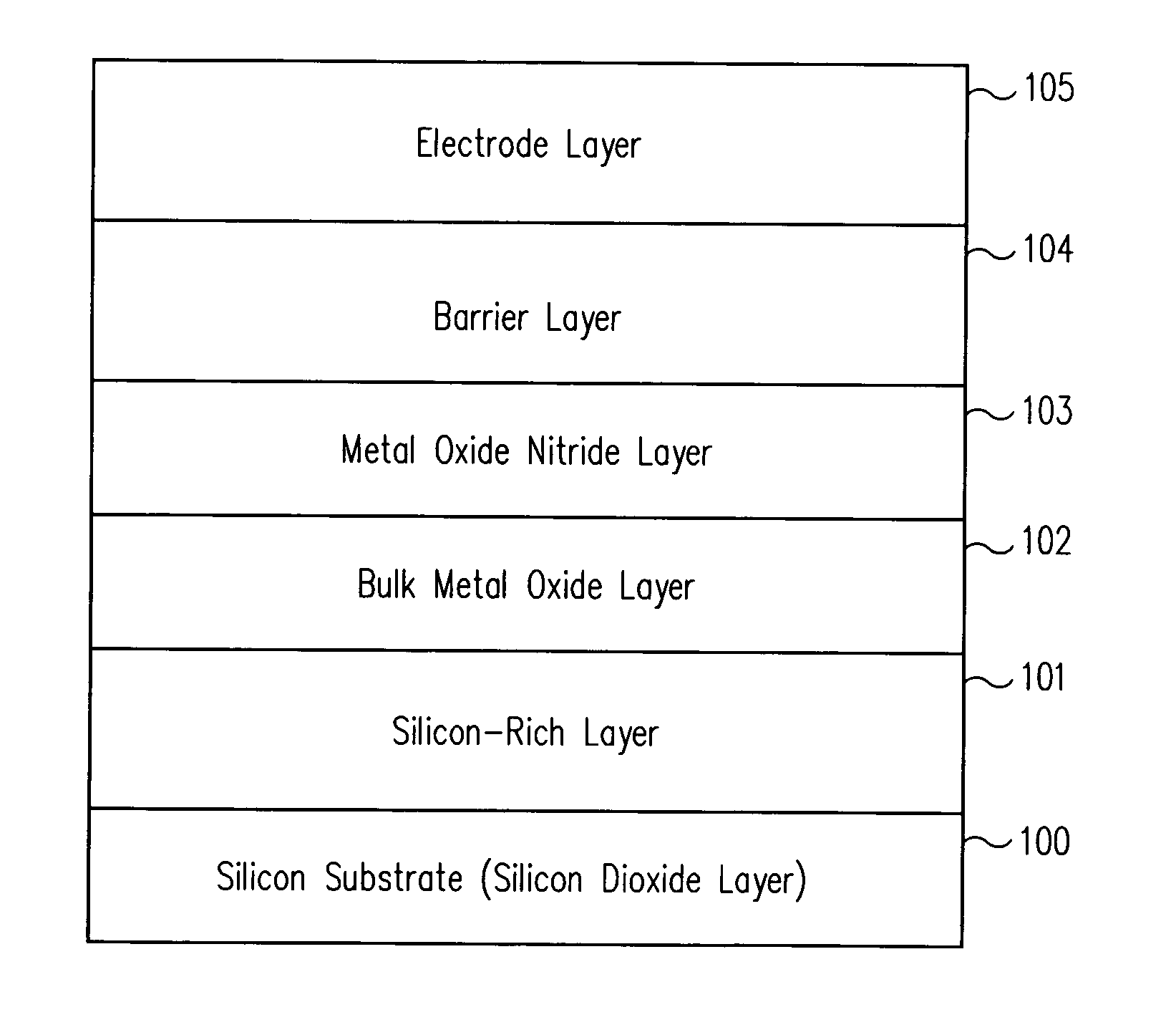
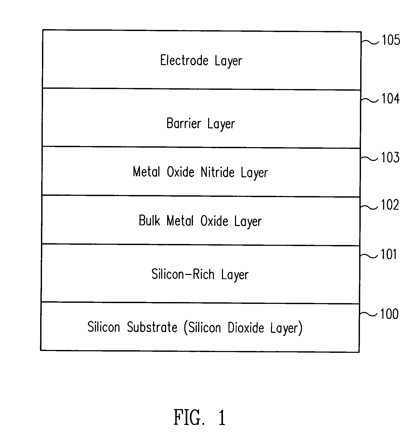
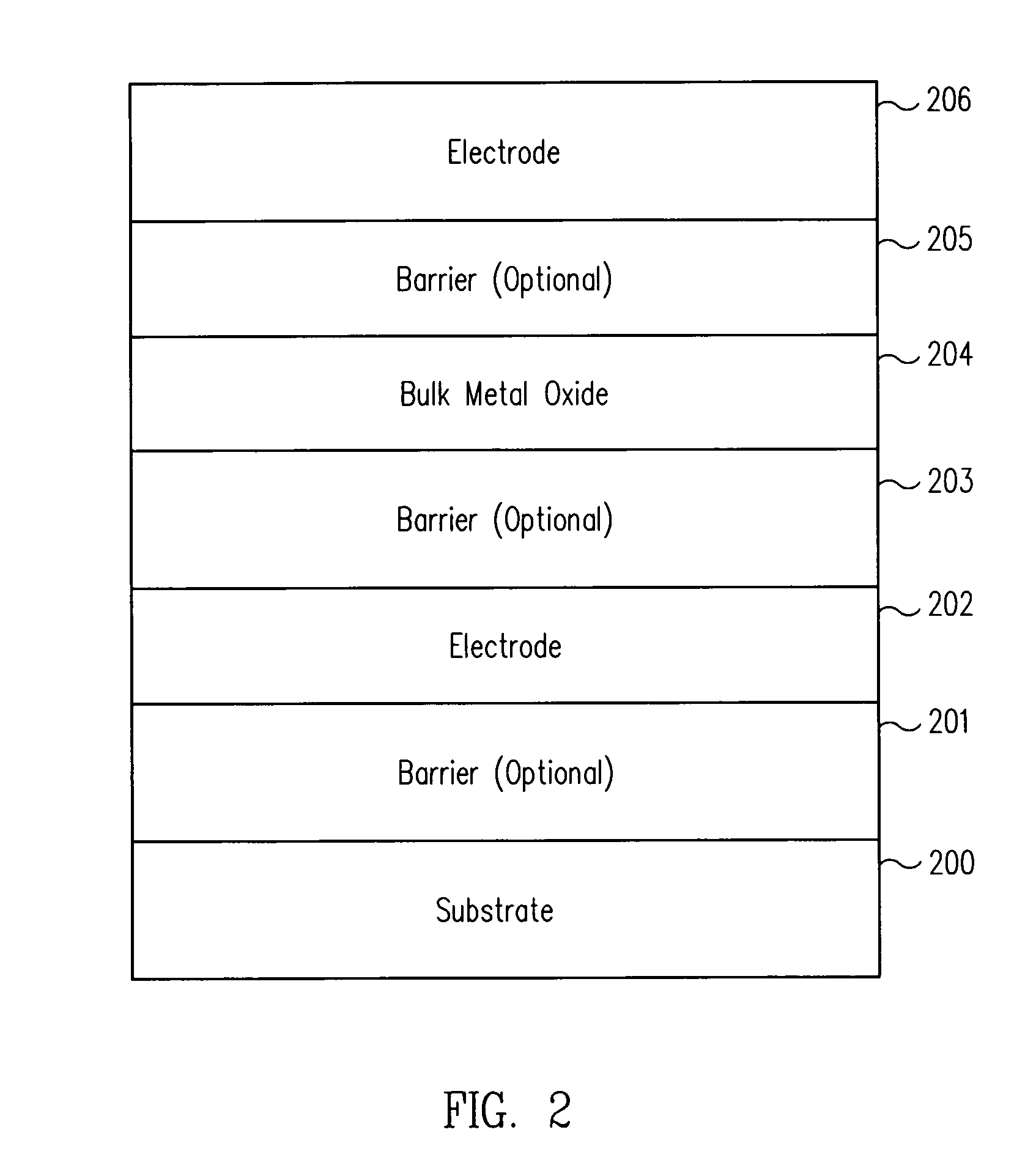
[0021] In general, the present invention provides for methods for deposition of a multi-component film material with a dielectric constant (high-k) higher than that of SiO2. The high-k material finds uses in the manufacture of semiconductor structures such as gates, capacitors, and the like. The methods provide for the introduction of a composition gradient throughout the film during the deposition process. The method of present invention is illustrated with embodiments where a silicon wafer is used as the substrate. It will be appreciated that the method may be used to deposit films on any suitable substrates such as silicon wafers, compound semiconductor wafers, glasses, flat panels, metals metal alloys, plastics, polymers organic materials, inorganic materials, and the like.

[0022] In one embodiment, the present invention provides a dielectric film comprising a composition of HfTiSixOyNz wherein x, y, and z represent a number from 0 to 2, respectively. The dielectric film may be ...


PUM

PropertyMeasurementUnit
Temperatureaaaaaaaaaa
Fractionaaaaaaaaaa

Abstract

The present invention provides systems and methods for forming a multi-layer, multi-component high-k dielectric film. In some embodiments, the present invention provides systems and methods for forming high-k dielectric films that comprise hafnium, titanium, oxygen, nitrogen, and other components. In a further aspect of the present invention, the dielectric films are formed having composition gradients.

Description

CROSS REFERENCE TO RELATED APPLICATIONS [0001] This application claims benefit of priority under 35 U.S.C. § 119(e) to U.S. Provisional Patent Application No. 60 / 669,812 filed Apr. 7, 2005, the disclosure of which is incorporated herein by reference in its entirety.FIELD OF THE INVENTION [0002] In general, the present invention relates to systems and methods for forming high-k dielectric films in semiconductor applications. More specifically, the present invention relates to systems and methods for fabricating multi-component dielectric films comprising hafnium, titanium, oxygen, nitrogen and other components on a substrate. BACKGROUND OF THE INVENTION [0003] The requirements for increased performance and speed provide some of the driving forces for the continuing scaling of microelectronic devices. Additionally, the expectations of higher performance, increased features, and lower costs from the end users provide a driving force to accomplish the scaling in an economic manner. Thes...

Claims


Application Information

Patent Timeline
IPC IPC(8): H01L21/31H01L23/58
CPCC23C16/308H01L29/518H01L21/28194H01L21/28202H01L21/3142H01L21/3143H01L21/3145H01L21/31604H01L21/31608H01L21/31637H01L21/31645H01L28/40H01L29/513H01L29/517C23C16/45523H01L21/02183H01L21/02266H01L21/0217H01L21/02161H01L21/02194H01L21/0228H01L21/02186H01L21/02153H01L21/0214H01L21/02145H01L21/02148H01L21/02181H01L21/31
Inventor BARTHOLOMEW, LARRY D.TREICHEL, HELMUTHOWYANG, JON S.
Owner AVIZA TECHNOLOGY INC
Why Eureka
Try Eureka