Laser-ablated fiber devices and method of manufacturing the same

a laser-ablated fiber and fiber technology, applied in the direction of manufacturing tools, instruments, optical elements, etc., can solve the problems of no commercial value, low stability of fiber couplers with respect to the environment, fatal shortcoming, etc., and achieve the effect of avoiding light loss and avoiding light loss

Inactive Publication Date: 2006-11-30
NAT CHIAO TUNG UNIV
View PDF11 Cites 28 Cited by
  • Summary
  • Abstract
  • Description
  • Claims
  • Application Information

AI Technical Summary

Benefits of technology

[0008] The main purpose of the present invention is to propose a manufacturing method of laser-ablated fiber devices. The cladding of the fiber is directly ablated by the laser so that an evanescent field of the fiber is exposed, wherein the ablation depth is estimated according to the distance between the interference fringes from another laser light. During the laser ablation, the fiber has to be kept bent so that the ablation depth of the cladding, where a depth is formed, gradually changes and thus a loss of the light is avoided. A length formed by ablating the fiber is controlled by varying the radius of curvature of the fiber. Besides, when the laser beam ablates a straight fiber, the traveling trajectory of the laser beam could be programmed so that any shape of the ablation on the cladding after can be designed and thus a loss of the light is avoided. This kind of laser-ablated fiber devices can be utilized to manufacture an evanescent wave fiber coupler, a fiber add / drop multiplexer, a fiber filter, a fiber polarizer, a fiber amplifier, and such active / passive fiber components as the fiber laser and fiber gratings.

Problems solved by technology

However, this kind of fiber coupler has low stability with respect to the environment and thus has no commercial value as a result of shortcomings like insufficiency in polished length, necessity of a refractive index matched liquid, and a high production cost therefore.
However, such a method has a fatal shortcoming, i.e. it fails to manufacture fiber devices at a high quality.
As long as the length of fused-tapering becomes longer, the phase difference between two polarization states will enormously increase due to birefringence of the coupling region, and thus the channel isolation of the fiber device becomes bad.
Accordingly, it is not easy to manufacture a fiber coupler with a narrow channel spacing and high channel isolation.
Besides, this method is not suitable for manufacturing low loss and polarization isotropic coarse-wavelength-division-multiplexing (CWDM) fiber couplers.
However, the technology they develop in polishing fibers utilizes a grinder, and it is necessary to add a thin film of sol-gel silica to fill in between the polished surfaces of the fibers when the fibers are fused.
Although the abovementioned method improves the stability of the side-polished fiber coupler, due to the deficient manufacture process and a tapering process not considered, the coupling ratio and wavelength coupling characteristics are not tunable.
Accordingly, this method is not practical.
However, the side-polished fiber devices lack the practical value in commercial use because the process of manufacturing side-polished fiber devices is time-consuming and they consume a large amount of polishing slurry and pads and precision silicon V-grooves.
However, it is obvious that a notch formed by the laser ablation to the fiber will lead to an abrupt change in the mode field distribution as a result of an abrupt change in thickness of the cladding and produce a phenomenon of coupling of high order mode, thereby resulting in severe optical losses of guiding lights.
Moreover, the ablation depth is judged by the power variations of the signal laser, and it is difficult to know the accurate remained cladding thickness since coupling efficiency of signal laser is so poor due to the mismatch between propagation constants of signal laser light and guiding lights in the ablated fiber.
Thus, this method cannot reflect an accurate ablation depth.
From the above description, it is known that how to develop a method of manufacturing laser-ablated fiber devices through the laser ablation has become a major problem to be solved.

Method used


Image

  • Laser-ablated fiber devices and method of manufacturing the same
  • Laser-ablated fiber devices and method of manufacturing the same
  • Laser-ablated fiber devices and method of manufacturing the same

Examples


Embodiment Construction

[0025] The present invention proposes a method for manufacturing laser-ablated fiber devices for different applications and will now be described more specifically with reference to the following embodiments. It is to be noted that the following descriptions of preferred embodiments of this invention are presented herein for purposes of illustration and description only; it is not intended to be exhaustive or to be limited to the precise form disclosed.

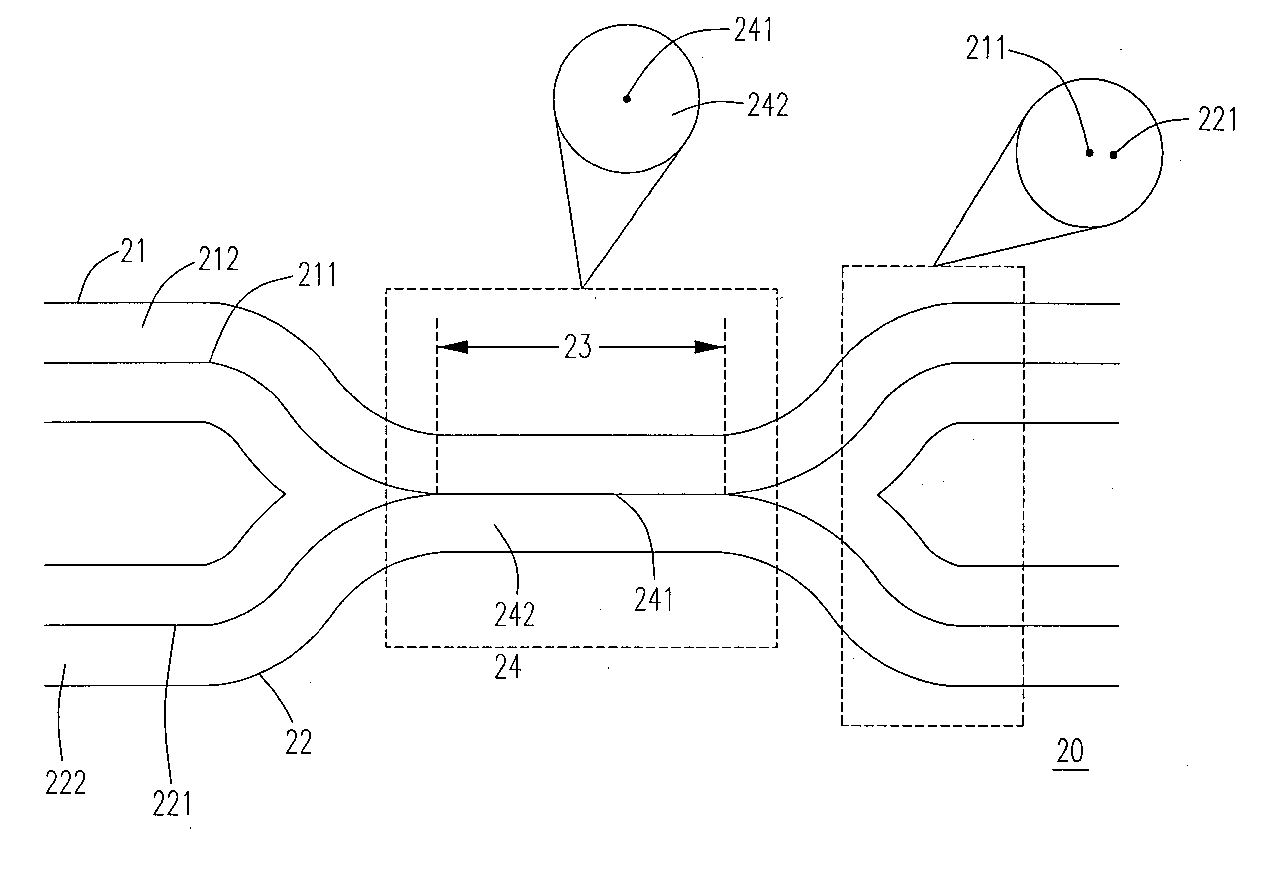
[0026] Please refer to FIG. 2, which is a schematic diagram showing the structure of the fiber coupler according to a preferred embodiment of the present invention. The method for manufacturing the fiber coupler 20 in FIG. 2 includes the following steps. Firstly, the fiber 21 and 22 are prepared, wherein the fiber 21 comprises the core 211 and the cladding 212, and the fiber 22 comprises the core 221 and the cladding 222. Next, a laser beam is utilized to respectively ablate the claddings 212 and 222 to form two evanescent field surf...


PUM

PropertyMeasurementUnit
evanescent fieldaaaaaaaaaa
depthaaaaaaaaaa
distanceaaaaaaaaaa

Abstract

A manufacturing method of a laser-ablated fiber device is proposed. The fiber cladding is removed by laser beam until the evanescent field is accessed. The depth of ablation is controlled by measuring the distance between the interference fringes of the laser. The effective interaction length is tuned by varying the radius of curvature of the fiber. The ablated fibers are mated to act as a fiber coupler. Subsequently, the interaction region is fused or fused-tapered to make a fiber coupler, an add / drop multiplexer, a fiber filter, etc.

Description

FIELD OF THE INVENTION [0001] The present invention relates to a method for manufacturing laser-ablated fiber devices. More particularly, the present invention relates to a method of manufacturing laser-ablated fiber devices through the laser ablation. BACKGROUND OF THE INVENTION [0002] The side-polished fiber coupler was first proposed by Lab. of Prof. Shaw, Stanford University. Referring to FIG. 1(a), the fiber 11 is buried in the quartz base plate 12, and the cladding of the fiber is polished so that there is a distance of several micro meters between the polished cladding and the core, and then the side-polished fiber device is mutually stacked to form the fiber coupler 13, as shown in FIG. 1(b). The fiber coupler has advantages of a low loss (<0.5 dB) and a tunable coupling ratio. However, this kind of fiber coupler has low stability with respect to the environment and thus has no commercial value as a result of shortcomings like insufficiency in polished length, necessity o...

Claims


Application Information

Patent Timeline
Patent Type & Authority Applications(United States)
IPC IPC(8): B23K26/00
CPCB23K26/032B23K26/0626B23K26/0643B23K26/0665B23K26/0823G02B6/29334B23K26/421G02B6/02147G02B6/2821G02B6/2835G02B6/29332B23K26/409B23K26/60B23K26/40B23K2103/172
Inventor CHI, SIENCHEN, NAN-KUANG
Owner NAT CHIAO TUNG UNIV
Why Eureka
Try Eureka