
Solder joints for copper metallization having reduced interfacial voids

Active Publication Date: 2006-11-30
TEXAS INSTR INC
View PDF12 Cites 19 Cited by
  • Summary
  • Abstract
  • Description
  • Claims
  • Application Information

AI Technical Summary

Benefits of technology

[0006] Applicants recognize a need for a straightforward solution to improve the reliability of direct copper / solder contacts. A careful investigation has been conducted to study the interface between copper and solder under the long term influence of elevated temperatures or repeated temperature cycles, commonly referred to as “aging”. This investigation has the conditions identified under which, after aging, a large amount of voids has formed at the interface between solder and copper, which greatly decreases the interfacial strength of the intermetallic joint.
[0009] The investigations of the applicants showed that by increasing the grain size of the copper layer, the rate of copper diffusion can be slowed, thus slowing the formation of voids. Copper layers are often formed by plating copper onto a thin seed layer, for example on a polymer film. Since copper plates nearly epitaxially, the grain size of the seed layer has to be increased, for instance by annealing through baking or through laser heating, before the plating step.

Problems solved by technology

If sufficient quantity of the first metal diffuses into the second, voids can result.
Thus, grain boundaries supply a ready source of atoms to IMC, resulting in depletion along the grain boundaries.

Method used


Image

  • Solder joints for copper metallization having reduced interfacial voids
  • Solder joints for copper metallization having reduced interfacial voids
  • Solder joints for copper metallization having reduced interfacial voids

Examples


Embodiment Construction

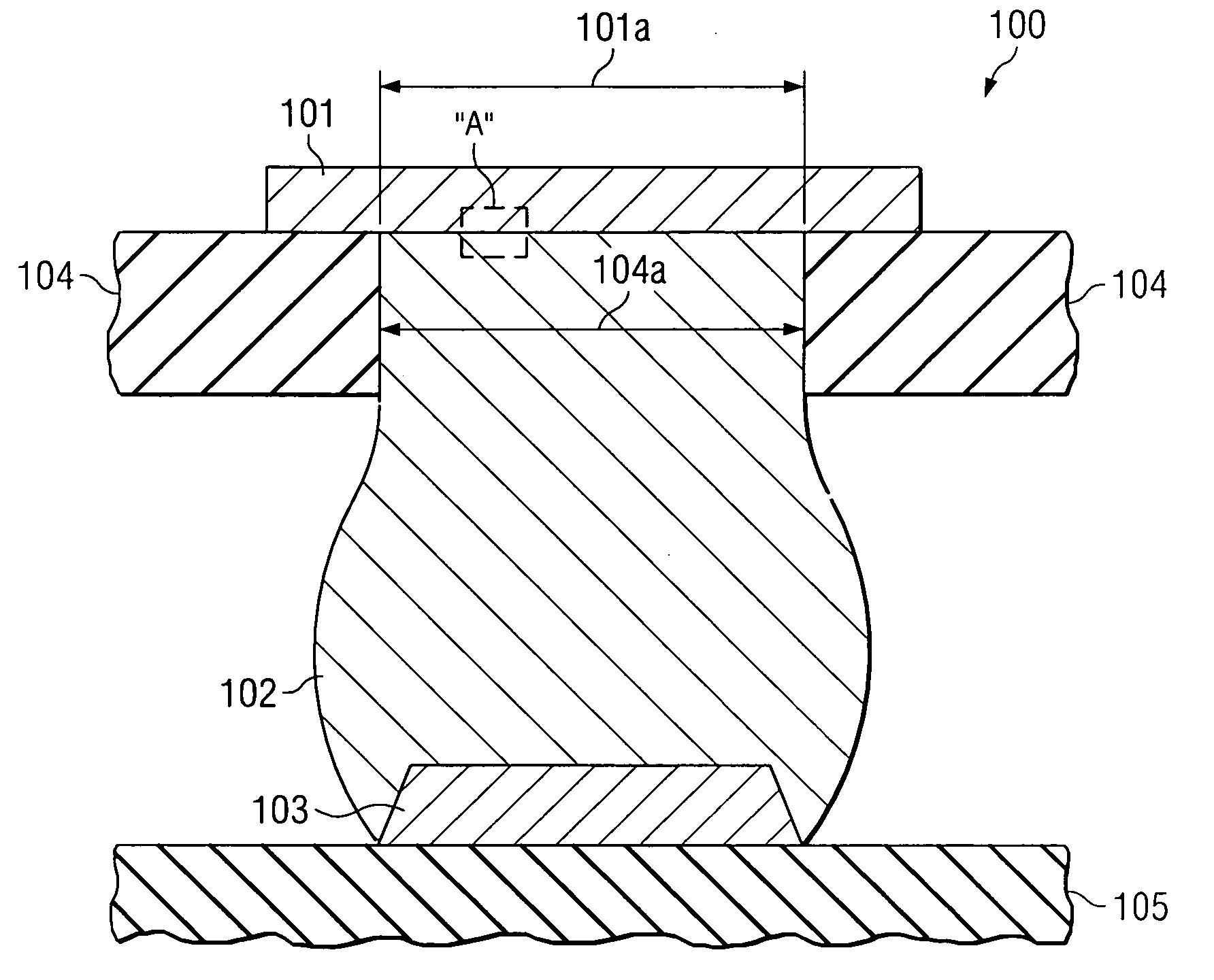
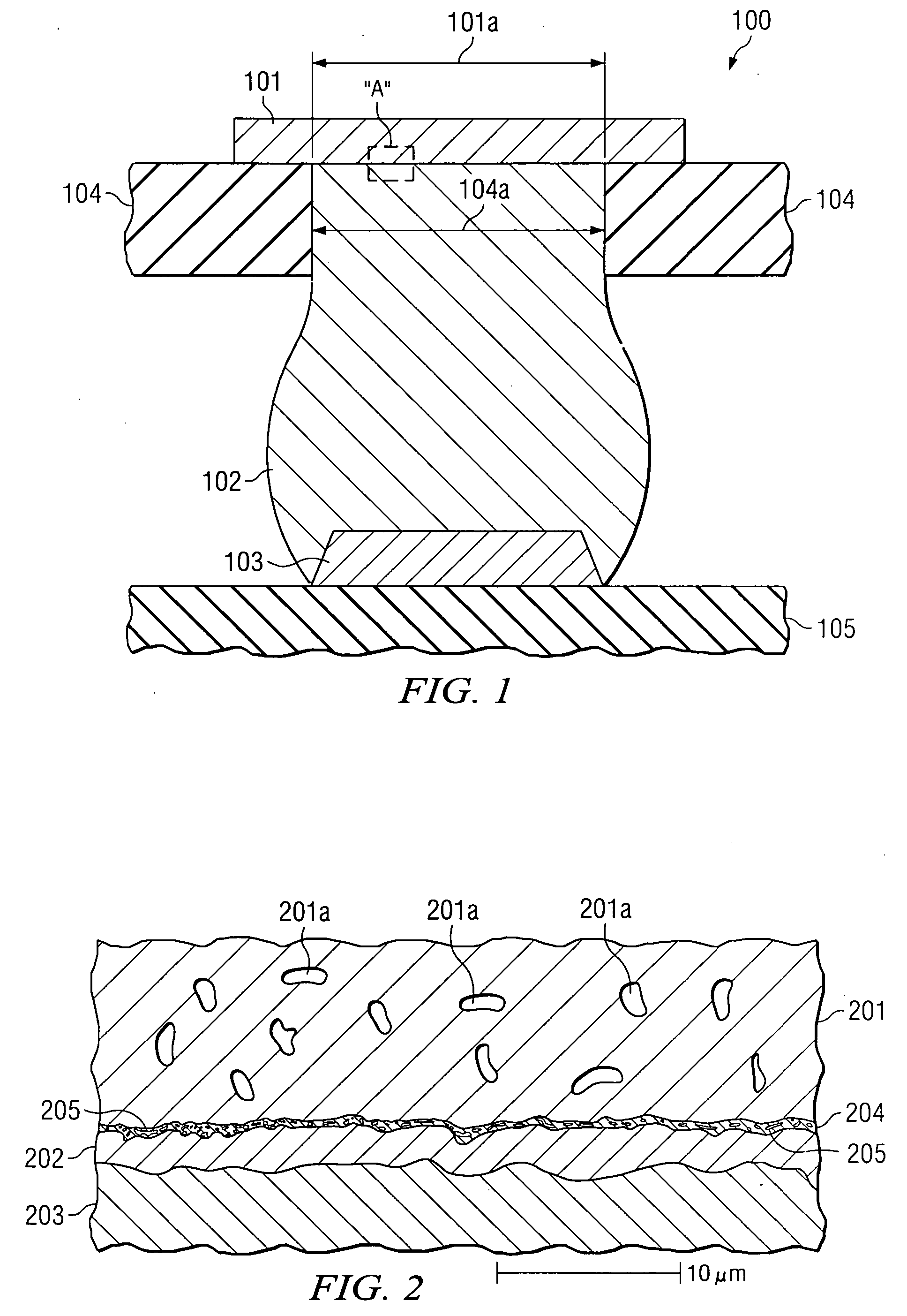
[0018] The schematic cross section of FIG. 1 illustrates an embodiment of the invention, a metal interconnect structure generally designated 100 as it is used in principle in many assemblies. The structure comprises a metal line 101, which provides the first contact pad 101a, a body of solder 102, and a second contact pad 103. At least one of the contact pads is made of copper; for example, if line 101 is made of copper, contact pad 101a is copper. In many embodiments, both contact pads of the interconnect structure are made of copper. In the example of FIG. 1, metal line 101 is supported by an insulating carrier 104. A window of width 104a in carrier 104 allows the solder of body 102 to be attached to the surface region of copper line 101 across pad width 101a. Contact pad 103 is also supported by a carrier, designated 105; frequently, carrier 105 is an external part, such as a printed circuit board made of insulating material.

[0019] The copper of line 101 and thus contact pad 101...


PUM

PropertyMeasurementUnit
Temperatureaaaaaaaaaa
Lengthaaaaaaaaaa

Abstract

A metal interconnect structure (100) comprising a bond pad (101), which has copper with at least 70 volume percent composed of crystal grains expanding more than 1 μm in their main direction, and 30 or less volume percent composed of crystal grains, which expand less than 1 μm in their main crystal direction. A body (102) of tin alloy is in contact with the bond pad.

Description

FIELD OF THE INVENTION [0001] The present invention is related in general to the field of semiconductor devices and more specifically to a structure and method of controlling metal interdiffusion and interfacial voids in solder interconnections in order to improve device reliability. DESCRIPTION OF THE RELATED ART [0002] When integrated circuits on semiconductor chips are to be interconnected to external circuitry on a substrate using reflow materials such as solder, the parts to be assembled have to undergo at least one temperature rise to above the melting temperature of the reflow material, followed by a cooling cycle. After completing this process, the finished assembly often has to be subjected to annealing steps, consisting typically of repeated temperature swings for an extended period of time. Finally, the assembled parts frequently have to be tested to determine their reliable functioning after repeated exposure to failure-accelerating conditions such as extreme temperature...

Claims


Application Information

Patent Timeline
IPC IPC(8): H01L23/58
CPCH01L21/4846Y10T428/24917H01L23/49866H01L24/10H01L2224/13099H01L2924/01013H01L2924/01029H01L2924/0103H01L2924/01033H01L2924/01049H01L2924/01078H01L2924/01079H01L2924/01082H01L2924/01322H01L2924/01327H01L2924/09701H01L2924/14H01L2924/15311H05K1/09H05K3/3436H05K2201/0394H05K2201/09472H05K2203/1105H01L2924/01006H01L2924/01047H01L2924/01087H01L2924/014H01L24/13H01L23/49816Y10T428/1291Y10T428/12715H01L2924/00H01L2924/181H01L2224/13Y02P70/50B32B15/08H01L23/532B32B15/20
Inventor EDWARDS, DARVIN R.CHIU, TZ-CHENGZENG, KEJUN
Owner TEXAS INSTR INC
Features
  • Generate Ideas
  • Intellectual Property
  • Life Sciences
  • Materials
  • Tech Scout
  • Unparalleled Data Quality
  • Higher Quality Content
  • 60% Fewer Hallucinations
Learn More