Methods of fabricating silicon carbide devices having smooth channels

a technology of silicon carbide and smooth channel, which is applied in the direction of semiconductor devices, basic electric elements, electrical apparatus, etc., can solve the problems of difficult to obtain the required depth of the p-base and nsup>+/sup> source regions using acceptable diffusion times and temperatures, and achieve the effect of reducing the surface roughness of the channel region

Active Publication Date: 2006-11-30
CREE INC
View PDF3 Cites 29 Cited by
  • Summary
  • Abstract
  • Description
  • Claims
  • Application Information

AI Technical Summary

Problems solved by technology

Notwithstanding these potential advantages, it may be difficult to fabricate power devices including power MOSFETs in silicon carbide.
Unfortunately, in silicon carbide, the diffusion coefficients of conventional p and n-type dopants are small compared to silicon, so that it may be difficult to obtain the required depths of the p-base and n+ source regions using acceptable diffusion times and temperatures.
However, it may be difficult to control the depth and lateral extent of ion implanted regions.
It may then be difficult to align the p-base and the source regions to one another, thereby potentially impacting the device performance.
Furthermore, performing a series implants and implant activation anneals may result in step bunched surfaces across the channel of the MOSFET, which may diminish device performance in terms of, for example, increased on resistance and reduced reliability.

Method used


Image

  • Methods of fabricating silicon carbide devices having smooth channels
  • Methods of fabricating silicon carbide devices having smooth channels
  • Methods of fabricating silicon carbide devices having smooth channels

Examples


Embodiment Construction

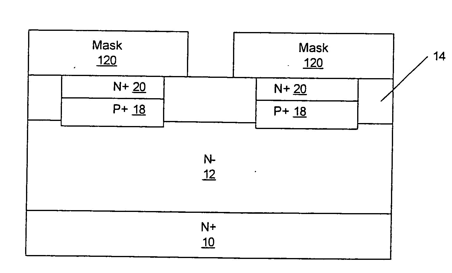
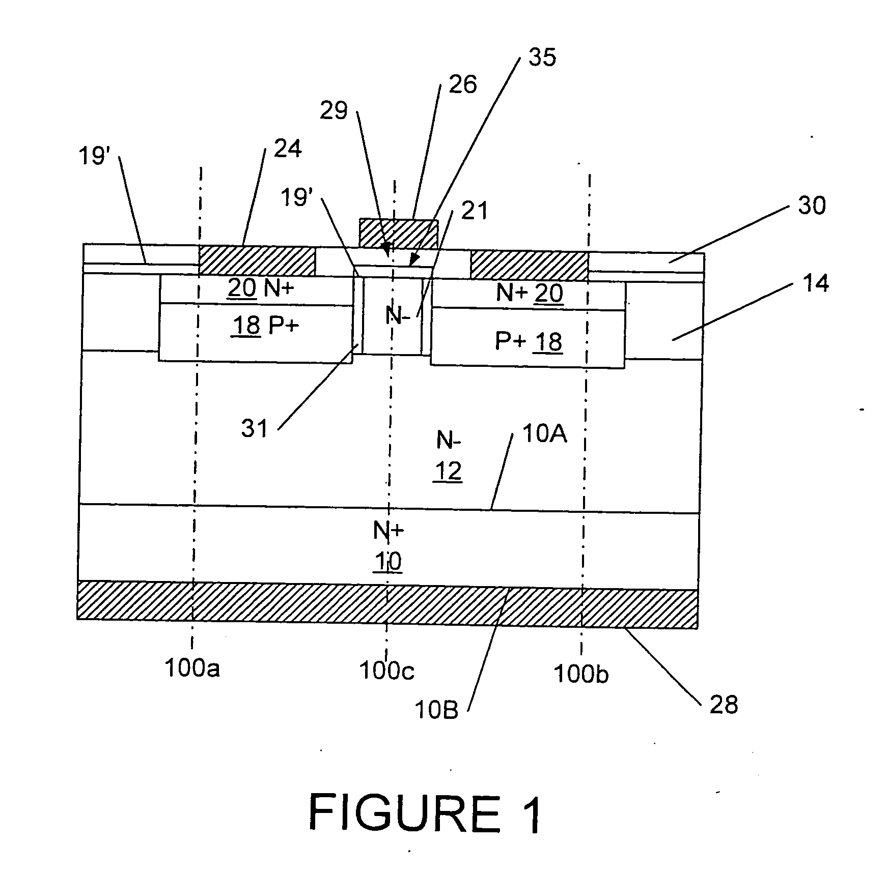
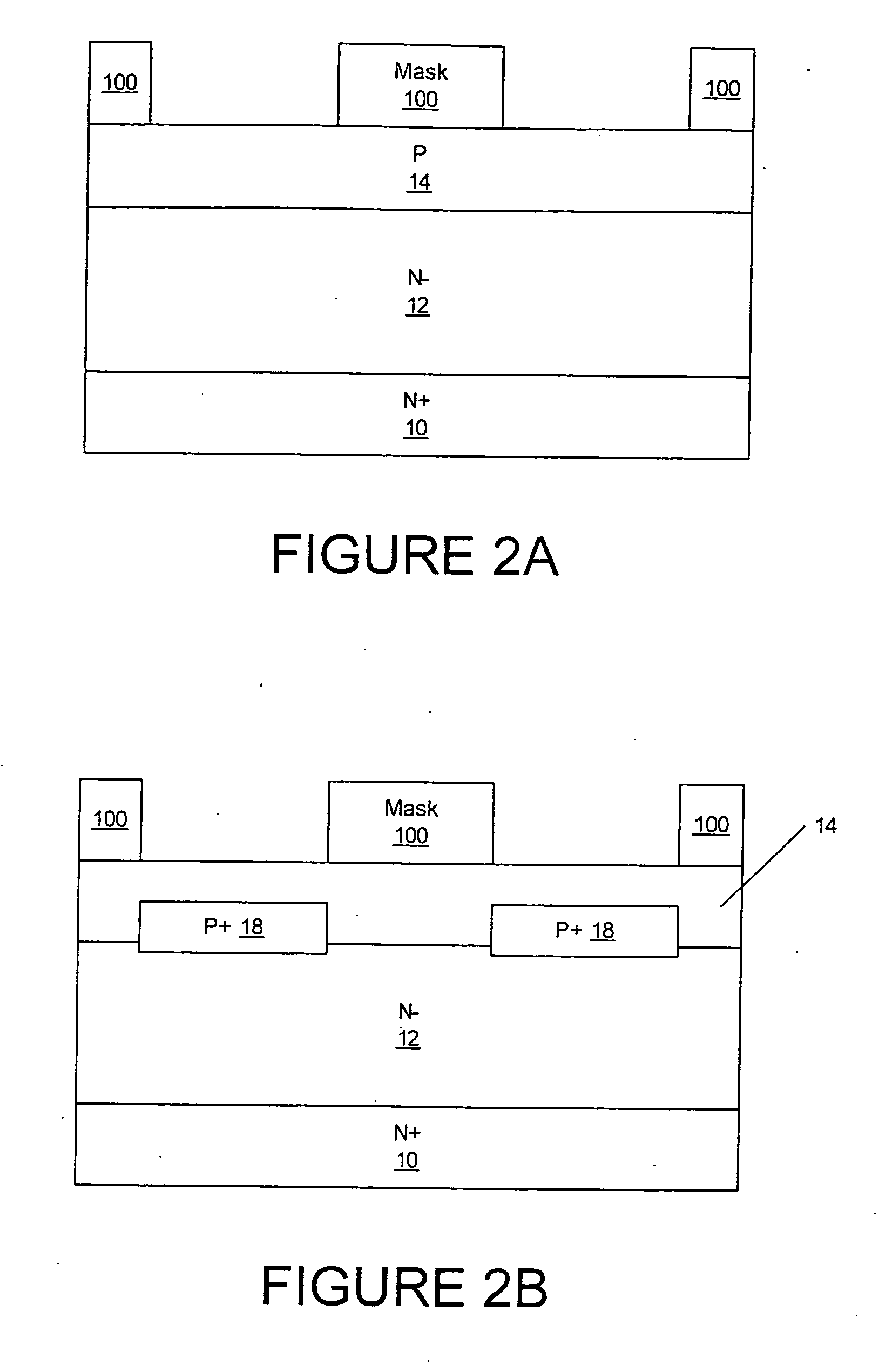
[0023] The present invention now will be described more fully hereinafter with reference to the accompanying drawings, in which embodiments of the invention are shown. This invention may, however, be embodied in many different forms and should not be construed as limited to the embodiments set forth herein. Rather, these embodiments are provided so that this disclosure will be thorough and complete, and will fully convey the scope of the invention to those skilled in the art. In the drawings, the size and relative sizes of layers and regions may be exaggerated for clarity. It will be understood that when an element or layer is referred to as being “on”, “connected to” or “coupled to” another element or layer, it can be directly on, connected or coupled to the other element or layer or intervening elements or layers may be present. In contrast, when an element is referred to as being “directly on,”“directly connected to” or “directly coupled to” another element or layer, there are no...


PUM

PropertyMeasurementUnit
temperatureaaaaaaaaaa
carrier concentrationaaaaaaaaaa
thicknessaaaaaaaaaa

Abstract

Methods of forming silicon carbide power devices are provided. An n− silicon carbide layer is provided on a silicon carbide substrate. A p-type silicon carbide well region is provided on the n− silicon carbide layer. A buried region of p+ silicon carbide is provided on the p-type silicon carbide well region. An n+ region of silicon carbide is provided on the buried region of p+ silicon carbide. A channel region of the power device is adjacent the buried region of p+ silicon carbide and the n+ region of silicon carbide. An n− region is provided on the channel region and a portion of the n− region is removed from the channel region so that a portion of the n− region remains on the channel region to provide a reduction in a surface roughness of the channel region.

Description

STATEMENT OF GOVERNMENT INTEREST [0001] The present invention was developed with Government support under contract number FA8650-04-2-2410 awarded by the United States Air Force. The Government has certain rights in this invention.FIELD OF THE INVENTION [0002] This invention relates to methods of fabricating power devices and the resulting devices and, more particularly, to silicon carbide power devices and methods of fabricating silicon carbide power devices. BACKGROUND OF THE INVENTION [0003] Power devices are widely used to carry large currents and support high voltages. Modern power devices are generally fabricated from monocrystalline silicon semiconductor material. One widely used power device is the power Metal Oxide Semiconductor Field Effect Transistor (MOSFET). In a power MOSFET, a control signal is supplied to a gate electrode that is separated from the semiconductor surface by an intervening insulator, which may be, but is not limited to, silicon dioxide. Current conduct...

Claims


Application Information

Patent Timeline
Patent Type & Authority Applications(United States)
IPC IPC(8): H01L21/00H01L21/336
CPCH01L29/0873H01L29/0886Y10S438/931H01L29/66068H01L29/7802H01L29/1608H01L29/0878
Inventor DAS, MRINAL K.LAUGHNER, MICHAEL
Owner CREE INC
Why Eureka
Try Eureka