Copper strike plating method

a technology of copper strike and copper plate, which is applied in the direction of semiconductor devices, semiconductor element details, electrical apparatus, etc., can solve the problems of lead frame mechanical characteristics such as press working performance, lead frame damage, etc., and achieve the effect of shortening the pretreatment steps

Inactive Publication Date: 2006-12-07
SHINKO ELECTRIC IND CO LTD
View PDF4 Cites 3 Cited by
  • Summary
  • Abstract
  • Description
  • Claims
  • Application Information

AI Technical Summary

Benefits of technology

[0015] The disclosure below describes a copper strike plating method, capable of shortening pretreatment steps as short as possible when a copper strike plating is applied to a substrate made of a copper alloy that was subjected to a heat treatment, and also forming a copper strike plating layer that is able to satisfy adequately an adhesiveness to the substrate and a heat resistance.
[0020] Also, the substrate made of the copper alloy that is formed by adding at least one element selected from a group consisting of Ni, Fe, Sn, Cr, Si and Mg to a matrix formed of copper is employed as the substrate. Therefore, machining performances such as the press working performance, and the like of the substrate can be improved.
[0022] Various implementations may include one or more the following advantages. For example, according to the copper strike plating method of the present disclosure, the degreasing process and the activating process are applied to the substrate made of the copper alloy that was subjected to the heat treatment, and then the copper strike plating is applied by applying a pulse current by which a current appears like a series of pulses only on the polarity side onto which the copper metal is deposited on the surface of the substrate. Therefore, the copper strike plating layer in which the metal crystals made of copper are densely filled can be formed on the surface of the substrate. The reason for this can be considered as follows.
[0027] In this manner, according to the copper strike plating executed by applying the pulse current by which the current appears like a series of pulses only on the polarity side onto which the copper metal is deposited on the surface of the substrate, the generation of the crystal nucleus is caused preferentially and uniformly in the substrate. Therefore, even when the surface of the substrate is in an uneven condition, the copper strike plating layer in which the metal crystals are densely filled and the adhesiveness to the substrate and the heat resistance of which are improved can be formed. As a result, the polishing process, and the like to be applied as the pretreatment steps prior to the strike plating can be omitted.

Problems solved by technology

When this plated thin film is peeled off from the lead frame by the heat load, in some cases an electrical connection between the semiconductor element and the lead frame is damaged.
As a result, mechanical characteristics of the lead frame such as the press working performance, and the like are now handled as an issue.
However, when the copper strike plating is applied to the lead frame made of the copper alloy, which underwent such heat treatment, by applying a DC current to form a thin copper strike plating layer (underlying copper plating layer) on the surface of the lead frame, and then an electrolytic plating layer of desired thickness is formed by the electroplating, a plating layer consisting of the copper strike plating layer and the electrolytic plating layer lacks adhesiveness to the lead frame and a heat resistance.
The reason for this phenomenon is that metals are contained in the copper alloy constituting the lead frame to exert a harmful influence upon the plating characteristic and thus the adhesiveness of the plating layer to the lead frame is deteriorated.
However, the pretreatment steps executed before the copper strike plating applied to the lead frame made of the copper alloy, which underwent the heat treatment, consumes much time.
Thus, the steps of manufacturing the lead frame become complicated and also a production cost of the lead frame is increased.
In this manner, the copper strike plating layer formed of large-sized metal crystals is inferior in the adhesiveness to the substrate and the heat resistance.
However, there is a limit to an adjustment of the surface of the substrate.
Thus, it is extremely difficult to form the copper strike plating layer having a dense structure.

Method used


Image

  • Copper strike plating method
  • Copper strike plating method
  • Copper strike plating method

Examples


example 1

[0064] The lead frame was obtained as the substrate by applying the press working to the stripe member made of the Cu—Ni—Si alloy (Corson alloy) that contains Mg at 0.15 wt %. Then, the heat treatment was applied to remove the machining distortion of the lead frame. Then, only the alkaline degreasing process and the electrolytic activating process were applied to this lead frame.

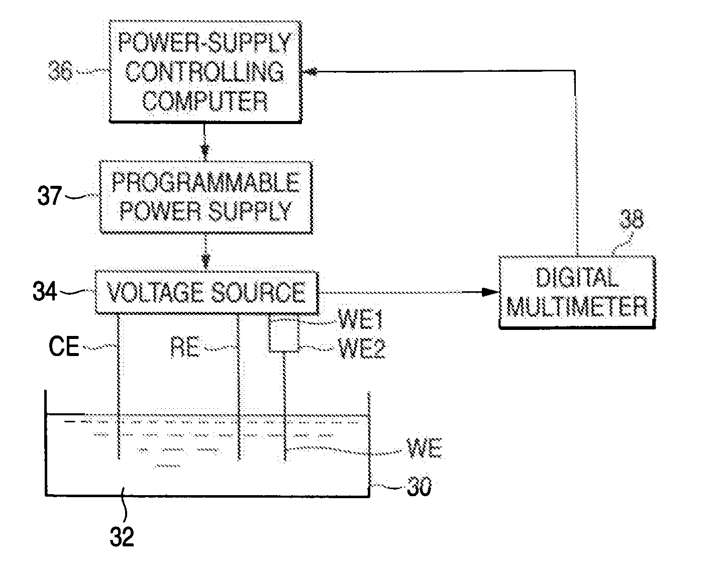
[0065] Then, while using the electrolytic copper plating equipment shown in FIG. 1, the lead frame was inserted as the substrate WE into the plating tab 30 in which an electrolytic copper plating solution is accumulated, and then the copper strike plating was applied to the surface of the lead frame by applying the pulse current.

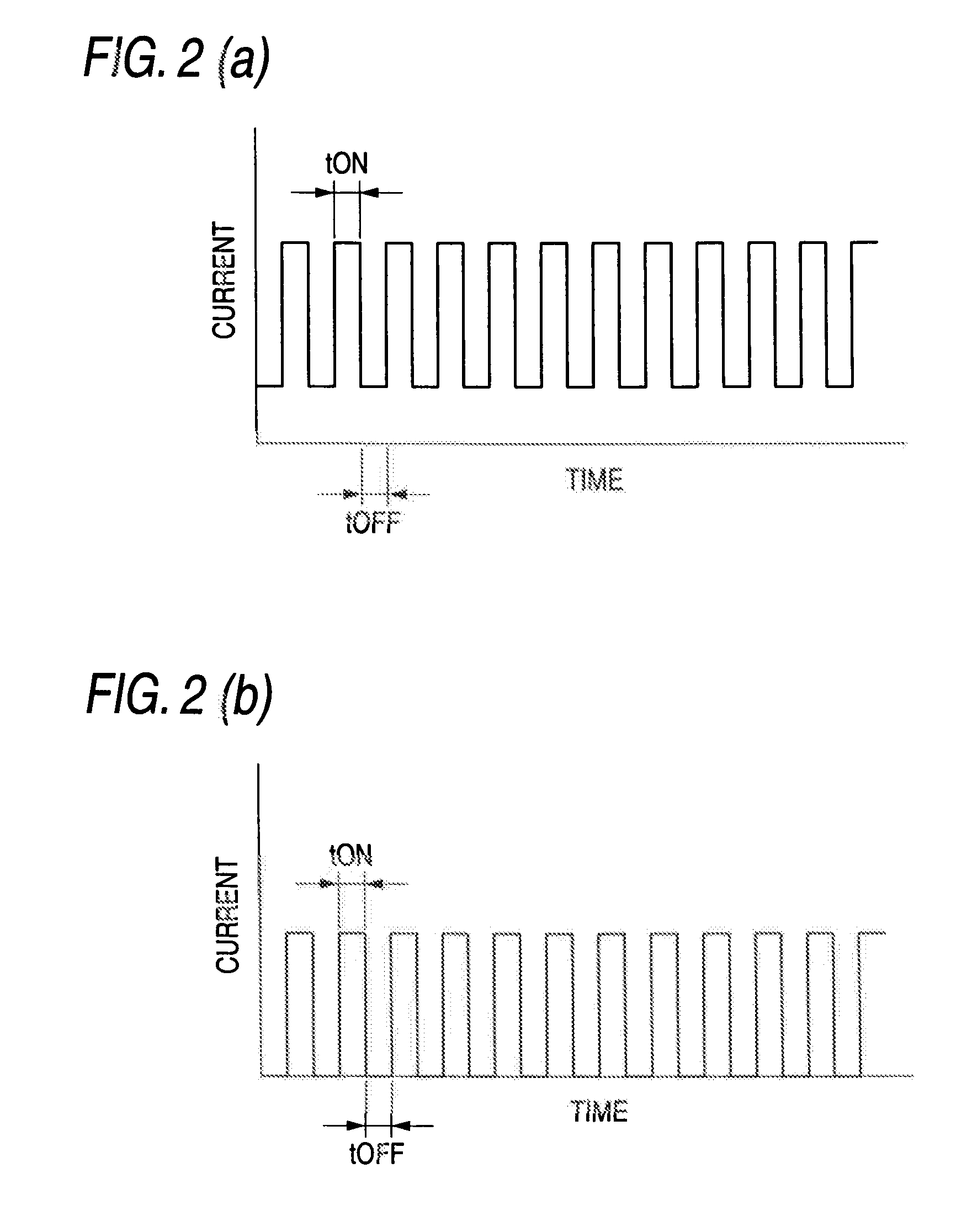
[0066] In the copper strike plating at this time, a pulse period of the pulse current was set to 100 Hz and also an average current density (C.D.) was set to 7 A / dm2. Then, the copper strike plating layer of 0.5 μm thickness was formed while changing the duty ratio from 0.2 to 1.0....

example 2

[0070] In Example 2, the copper strike plating and the electrolytic silver plating were applied in the similar manner to Example 1 except that the pulse period was changed as shown in Table 2 while keeping the duty ratio at 0.4. The results of the visual observation about the appearance of the copper strike plating layer and the appearance of the silver plating layer and occurring extents of nodule (surface roughness), level difference, and unevenness of gloss indicating the Ag anomalous deposition are also given in Table 2. In Table 2, ◯ denotes good, Δ denotes that the anomalous deposition was recognized slightly, and X denotes that the anomalous deposition was recognized.

TABLE 2Ag Anomalous DepositionPeriodAppearanceAppearanceUn-No.(Hz)of Cu layerof Ag layerNoduleL.D.evenness11◯◯◯◯◯210◯◯◯◯◯3100◯◯◯◯◯41000◯◯◯◯◯

[0071] As apparent from Table 2, even though the polishing was not applied to the lead frame that was subjected to the heat treatment, the good copper strike plating layer ...

example 3

[0074] In Example 3, the plating was applied to the lead frame by setting other conditions similarly to Example 1 except that the copper strike plating layer of 0.1 μm thickness was formed by applying the copper strike plating under conditions that the pulse period of the pulse current supplied to the lead frame was set to 100 Hz, the average current density (C.D.) was set to 7 A / dm2, and the duty ratio was set to 0.4 and that the silver plating layer of 3 to 5 μm thickness was formed on this copper strike plating layer by the electrolytic silver plating.

[0075] Then, a copper oxide film was formed on the lead frame that was subjected to the plating under the heating condition given in Table 3, and then a tape peeling test to check whether or not the plating layer is peeled off was executed by peeling off an adhesive tape stuck on the lead frame. In this manner, the adhesiveness of the copper strike plating layer to the oxide film was evaluated. The results of the evaluation are als...


PUM

PropertyMeasurementUnit
thicknessaaaaaaaaaa
current efficiencyaaaaaaaaaa
average current densityaaaaaaaaaa

Abstract

Upon applying a copper strike plating to a surface of a substrate made of a copper alloy that was subjected to a heat treatment after a degreasing process and an electrolytic activating process are applied to the surface, a pulse current by which a current appears like a series of pulses only on a polarity side onto which a copper metal is deposited on the surface of the substrate is applied to the substrate in the copper strike plating such that a crystal plane showing a maximum value of an X-ray diffraction intensity of a copper strike plating layer formed on the surface of the substrate corresponds to a (111) plane as a crystal plane showing a maximum value of an X-ray diffraction intensity of the copper layer into which metal crystals made of copper are most densely filled.

Description

TECHNICAL FIELD [0001] The present disclosure relates to a copper strike plating method. More particularly, the present disclosure relates to a copper strike plating method of applying a copper strike plating to a surface of a substrate made of a copper alloy that was subjected to a heat treatment after a degreasing process and an activating process are applied to the surface. RELATED ART [0002] In order to improve a bonding ability of the lead frame to the semiconductor element via the wire, and the like, the plating is applied to the lead frame used in the semiconductor device. [0003] In the step of mounting the semiconductor element onto the lead frame, the step of bonding the wire, and the like, a heat load is applied to a plated thin film that is formed on the lead frame by such plating. When this plated thin film is peeled off from the lead frame by the heat load, in some cases an electrical connection between the semiconductor element and the lead frame is damaged. For this r...

Claims


Application Information

Patent Timeline
Patent Type & Authority Applications(United States)
IPC IPC(8): H01L21/00
CPCC25D5/18C25D5/34H01L23/49582H01L2924/0002H01L2924/00C25D5/627C25D5/617C25D5/605C25D5/611
Inventor OGIHARA, YOKO
Owner SHINKO ELECTRIC IND CO LTD
Why Eureka
Try Eureka