Nanotube articles with adjustable electrical conductivity and methods of making the same

a technology of electrical conductivity and nanotubes, applied in the direction of fixed capacitor details, semiconductor/solid-state device details, weaving, etc., can solve the problem of reducing the electrical resistance of the layer of nanostructure, and achieve the effect of modifying the conductivity of the insulating nanotube fabri

Inactive Publication Date: 2006-12-07
NANTERO
View PDF21 Cites 113 Cited by
  • Summary
  • Abstract
  • Description
  • Claims
  • Application Information

AI Technical Summary

Benefits of technology

[0015] Under another aspect, exposure to the reactive ions increases the electrical resistance of substantially each individual nanostructure within the layer. Exposure to the reactive ions may increase the electrical resistance of the layer of nanostructures by a factor of at least 10. The layer of nanostructures may include a non-woven fabric of nanostructures. Each individual nanostructure within the layer may lie substantially parallel to a substrate. The nanostructures may include single-walled carbon nanotubes. The nanostructures may include multi-walled carbon nanotubes. The nanostructures may include nanowires. Heating the layer of nanostructures may reduce the electrical resistance of the layer of nanostructures.
[0018] Under another aspect, the non-woven fabric of nanotubes forms an electrical insulator. The electrical resistance of the fabric may be a function of a number of functional groups attached to substantially each individual nanotube of the fabric. Reaction of the fabric with reactive ions may at least partially functionalize substantially each individual nanotube of the fabric. Heating of the fabric may at least partially drive functional groups off of substantially each individual nanotube of the fabric. Heating of the fabric may reduce the electrical resistance of the fabric below about 10,000 Ω / square.

Problems solved by technology

Heating the layer of nanostructures may reduce the electrical resistance of the layer of nanostructures.

Method used


Image

  • Nanotube articles with adjustable electrical conductivity and methods of making the same
  • Nanotube articles with adjustable electrical conductivity and methods of making the same
  • Nanotube articles with adjustable electrical conductivity and methods of making the same

Examples


example 1

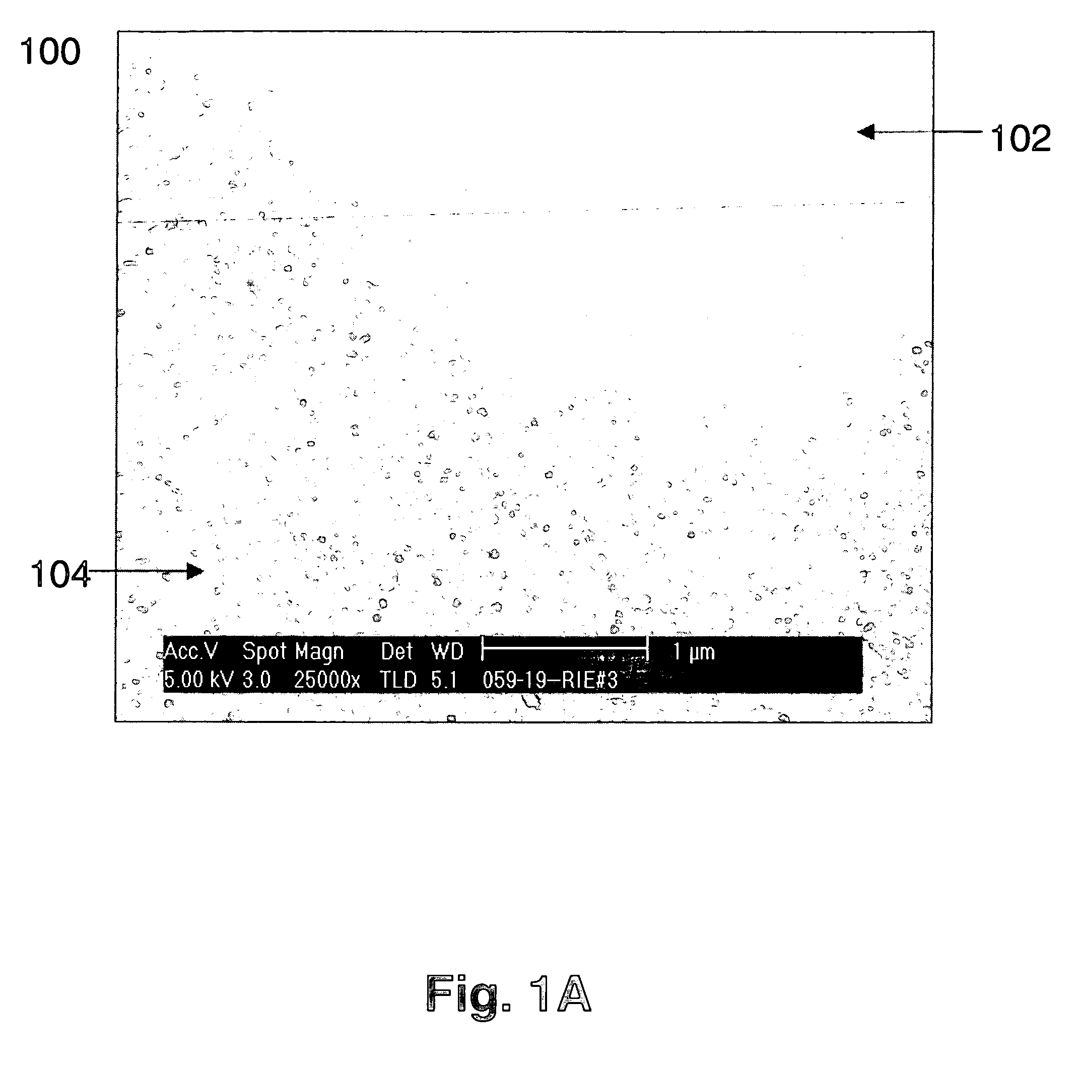
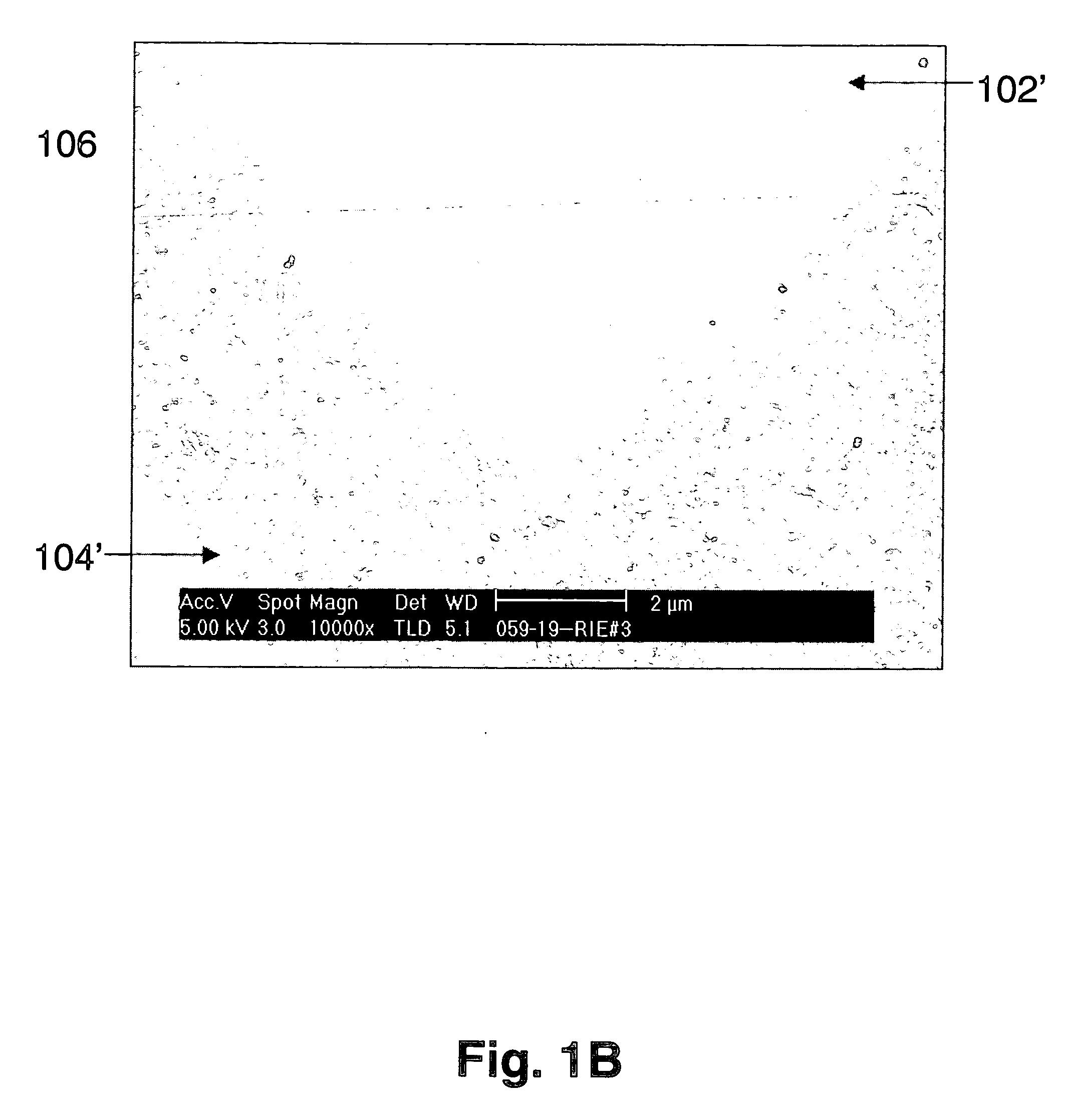
[0088] A layer of carbon nanotubes from several nanometers up to a micron thick is applied to a substrate either by spray coating, spin coating, dip coating, etc. The carbon nanotubes are then exposed to a gas that provides reactive ions, e.g., CF4, CHF3, H2, CH4, SF6, Ar, BCl3, Cl2, CCl2F2, SiCl4, C4F8, HBr, and mixtures thereof, as described in greater detail above, in a reactive ion etch chamber. The reactive ions react with the carbon nanotubes, modifying the nanotubes' electrical conductivity. The nanotube layer can be converted to a high resistance nanotube layer, or it can be converted to an intermediate resistance nanotube layer. Selection of plasma power in the RIE chamber, reactive ion density and reaction time, can minimize morphological damage of the CNT fabric while modifying the electrical properties as desired. As an example, a carbon nanotube fabric is sprayed onto a substrate to produce a low Ohm resistance fabric (4 gas is introduced at a pressure of 15 mTorr. The ...

example 2

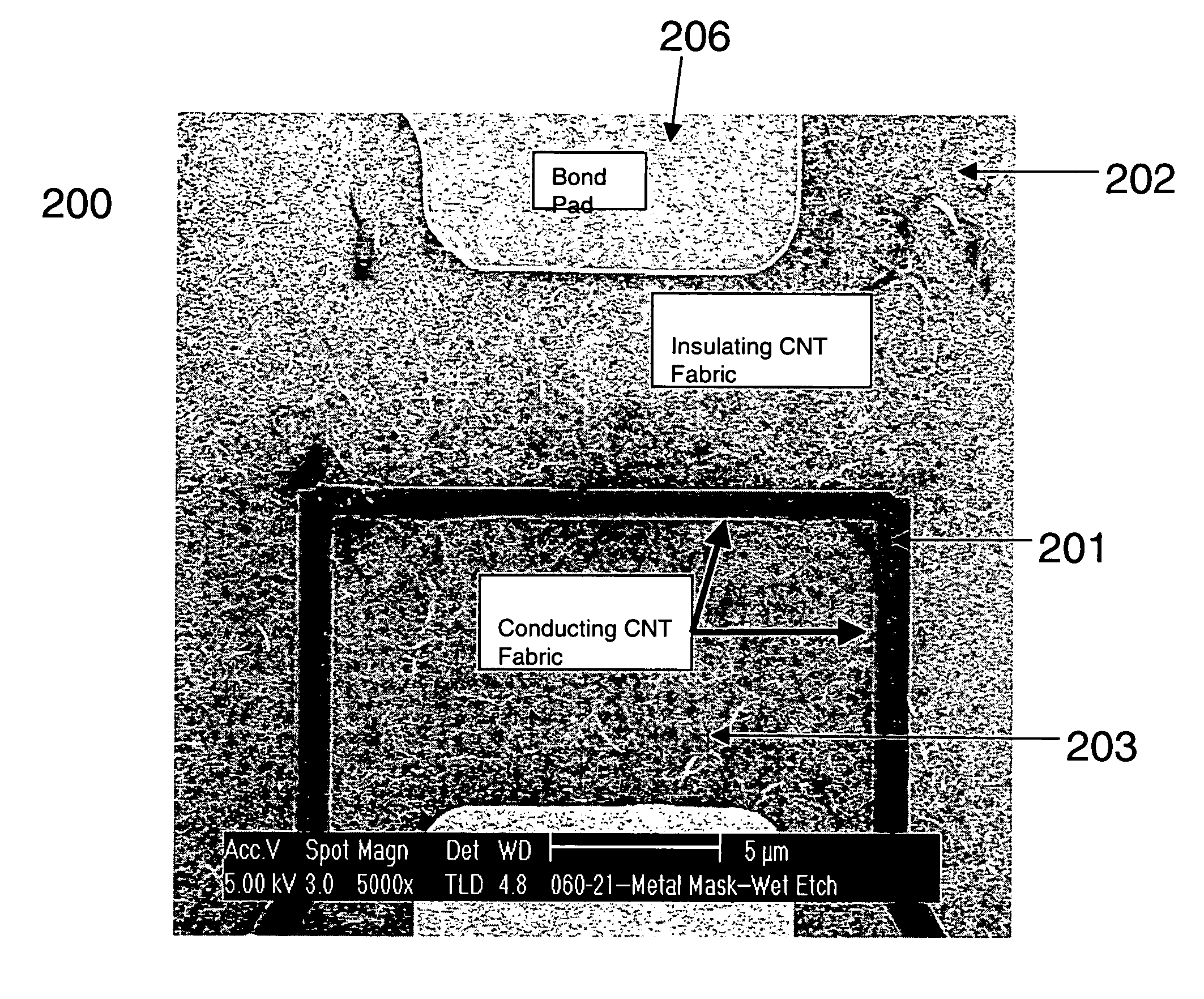
[0089] The steps of Example 1 are repeated, and then, a mask pattern is fabricated on top of the CNT fabric by spinning, exposing and developing photoresist. The substrate containing the CNT fabric was exposed to RIE plasma (containing CF4 gas at 30 mTorr at 30 Watts for 30 seconds). Unprotected portions of the CNT fabric were fully converted to an insulating fabric, while the mask prevented the underlying portion from being converted to a non-conducting CNT fabric. After RIE plasma exposure, the patterned mask was removed, leaving a defined region of patterned conducting CNT fabric within an insulating CNT fabric.

Other Embodiments

[0090] An alternate embodiment involves the creation of dielectric features of carbon nanotubes (CNTs) and nanotubes from a fabric initially including conducting nanotubes, or a mixture of conducting and semiconducting nanotubes.

[0091] In another embodiment, pinning of nanotubes onto the supports using an overlaid thin coating is done to prevent slippin...


PUM

PropertyMeasurementUnit
electrical resistanceaaaaaaaaaa
resistanceaaaaaaaaaa

Abstract

Nanotube articles having adjustable electrical conductivity, and methods of making the same. A patterned article includes conducting nanotubes that define a plurality of conductive pathways along the article, and also includes nanotubes of modified electrical conductivity. The modified nanotubes may electrically isolate the conducting nanotubes from other conductors. The nanotube segments may originally be semiconducting nanotubes, metallic nanotubes, nanotubes, single walled carbon nanotubes, multi-walled carbon nanotubes, or nanotubes entangled with nanotubes. The various segments may have different lengths and may include segments having a length shorter than the length of the article. A strapping material may be positioned to contact a portion of the plurality of nanotube segments. Such a strapping layer may also be used for making electrical contact to the nanotube fabric especially for electrical stitching to lower the overall resistance of the fabric.

Description

CROSS-REFERENCE TO RELATED APPLICATIONS [0001] This application claims the benefit under 35 U.S.C. § 19(e) of the following applications, the entire contents of which are hereby incorporated by reference herein: [0002] Patterned Nanoscopic Articles and Methods Of Making The Same (U.S. Provisional Patent Appln. No. 60 / 668,396), filed on Apr. 5, 2005; and [0003] Encapsulation of Metal Lines Within Dielectric CNT Fabric (U.S. Provisional Patent Appln. No. 60 / 714,282), filed on Sep. 6, 2005. [0004] This application is related to the following patent applications, which are assigned to the assignee of this application, and are hereby incorporated by reference in their entirety: [0005] Patterned Nanoscopic Articles and Methods of Making Same (U.S. patent application Ser. No. 10 / 936,119), filed on Sep. 8, 2004; [0006] Methods of Nanotube Films and Articles (U.S. Pat. No. 6,835,591), filed on Apr. 23, 2002; and [0007] Non-Volatile Electromechanical Field Effect Devices and Circuits Using Sa...

Claims


Application Information

Patent Timeline
Patent Type & Authority Applications(United States)
IPC IPC(8): D04H1/00H01L21/00D04H3/00D04H5/00
CPCB82Y10/00H01L2221/1094B82Y40/00C01B31/0253C01B31/0293C01B2202/02C01B2202/06C01B2202/22H01C17/0652H01G4/06H01L21/76801H01L21/76823H01L21/76828H01L21/76838H01L21/76888H01L23/53276H01L23/5329H01L27/0802B82Y30/00C01B32/168C01B32/18H01L2924/0002Y10T442/614Y10T442/615Y10T442/696Y10T442/697H01L2924/00
Inventor WARD, JONATHAN W.RUECKES, THOMASSEGAL, BRENT M.
Owner NANTERO
Why Eureka
Try Eureka