Silicon-based backward diodes for zero-biased square law detection and detector arrays of same

a backward diode and zero-biased square law technology, applied in the field of optical detectors, radiometers, imagers, can solve the problems of increasing system and pixel complexity, extra noise and drift, and devices not readily amenable to imaging applications, so as to reduce the height of the tunneling barrier

Active Publication Date: 2006-12-21
THE OHIO STATES UNIV +1
View PDF2 Cites 34 Cited by
  • Summary
  • Abstract
  • Description
  • Claims
  • Application Information

AI Technical Summary

Problems solved by technology

However, the biasing circuit greatly increases the system and pixel complexity and also leads to extra noise and drift.
However, because of the chosen substrates (germanium substrates for Ge backward diodes and GaAs substrates for planar-doped barrier GaAs diodes), these devices are not readily amenable to imaging applications, where a mass-producible technology is required to fabricate a large number of identical devices into compact pixelated imaging arrays.
However, the high cost of Sb-based backward diodes and their incompatibly with main-stream silicon read-out circuitry are problematic.

Method used


Image

  • Silicon-based backward diodes for zero-biased square law detection and detector arrays of same
  • Silicon-based backward diodes for zero-biased square law detection and detector arrays of same
  • Silicon-based backward diodes for zero-biased square law detection and detector arrays of same

Examples


example 1

Si / SiGe Backward Diode

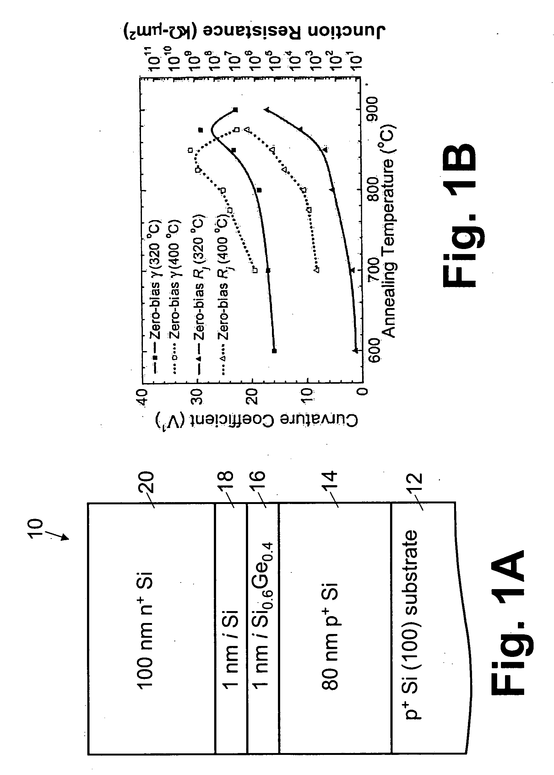
[0022] With reference to FIG. 1A, a Si-based backward diode structure 10 was fabricated. The Si-based backward diode structure 10 is a step p-i-n structure formed on a p+ Si (100) substrate 12 and includes an 80 nm boron (B)-doped p+ Si layer 14, an active region including a 1 nm Si0.6Ge0.4 layer 16 and a 1 nm Si layer 18, and a 100 nm phosphorous (P)-doped n+ Si cap layer 20. The active region layers 16, 18 are nominally undoped. Without being limited to any particular theory of operation, it is believed that the SiGe layer 16 reduces the tunnel barrier height, to enhance the momentum mixing, and hence to reduce the junction resistance.

[0023] Several samples of the structure 10 of FIG. 1A were grown by molecular beam epitaxy (MBE), using elemental Si and Ge in electron-beam sources. The substrates 12 were 75 mm B-doped (ρ=0.015-0.04Ω·cm) Si (100) wafers. The nominal doping levels for both the p-side 14 and n-side 20 are 5×1019 cm−3. Two structures were grown...

example 2

Si / SiGe Backward Diode with Delta-Doping

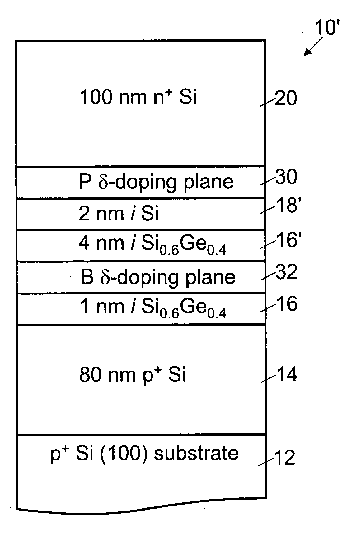
[0033] With reference to FIG. 3, samples of a modified Si-based backward diode structure 10′ were also fabricated. The structure of FIG. 3 differs from that of FIG. 1A in that it includes an n-type (phosphorus) delta doping 30 adjacent the 100 nm phosphorous (P)-doped n+ Si cap layer 20, and a p-type (boron) delta doping 32 adjacent the 1 nm nominally undoped Si0.6Ge0.4 layer 16. The 1 nm Si layer 18 is increased in thickness to a 2 nm Si layer 18′ disposed between the delta dopings 30, 32, and an additional 4 nm (nominally undoped) Si0.6Ge0.4 layer 16′ is also disposed between the delta dopings 30, 32. Although not shown, in some embodiments a second phosphorus delta doping is disposed at or near the top (exposed) surface of the phosphorus (P)-doped n+ Si cap layer 20 to reduce contact resistance. Alternatively, Ge doping or another technique for reducing contact resistance can be employed.

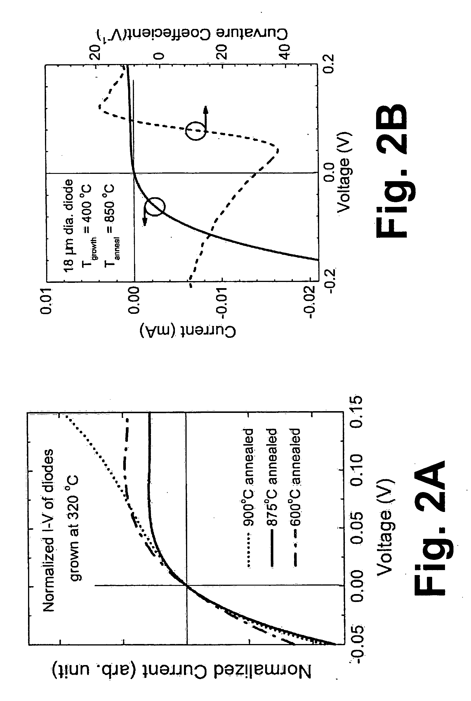
[0034] With reference to FIG. 4, I-V plots are show...

example 3

Asymmetric Si / SiGe Backward Diode with Delta-Doping

[0038] For example, FIG. 6A shows a contemplated Si-based backward diode structure 100 that is modified respective to the structure 10′ of FIG. 3. The structure of FIG. 6A differs from that of FIG. 3 in that a thicker ˜800 nm bottom p+ silicon layer 140 and 2 nm SiGe layers 160, 161 having a higher germanium fraction of 0.5 and having symmetric 2 nm thicknesses symmetrically sandwiching the p-type (boron) delta doping 32. Additionally, the bottommost SiGe layer 160 is doped p+.

[0039] The zero bias band structure for the structure 100 is shown in FIG. 6B. Although not shown, in some embodiments a second phosphorus delta doping is disposed at or near the top (exposed) surface of the phosphorus (P)-doped n+ Si cap layer 20 to reduce contact resistance. Alternatively, Ge doping or another technique for reducing contact resistance can be employed. FIG. 6B diagrammatically shows an estimated zero bias band structure in the vicinity of t...


PUM


Abstract

A Si-based diode (10, 10′, 100) is formed by epitaxially depositing a Si-based diode structure on a silicon substrate. The Si-based diode structure includes a Si-based pn junction (16, 16′, 18, 18′, 30, 32, 160, 161) having a backward diode current-voltage characteristic in which the forward tunneling current is substantially smaller than the backward tunneling current at comparable voltage levels. In some embodiments, the Si-based pn junction includes at least one non-silicon or silicon alloy layer such as at least one SiGe layer (16, 16′, 160, 161). In some embodiments, at least one delta doping (30, 32) is disposed on the silicon substrate in or near the pn junction, that together with the Si-based pn junction define an electrical junction having the backward diode current-voltage characteristic. A large area detector array may include a plurality of such Si-based diodes (10, 10′, 100).

Description

[0001] This application claims the benefit of U.S. Provisional Application No. 60 / 672,833 filed Apr. 19, 2005. U.S. Provisional Application No. 60 / 672,833 filed Apr. 19, 2005 is incorporated by reference herein in its entirety.[0002] This invention was made with Government support under NSF grant no. ESC-0323657 awarded by the National Science Foundation (NSF). The Government has certain rights in this invention.BACKGROUND [0003] The following relates to optical detectors, radiometers, imagers, and so forth. It finds particular application in conjunction with silicon-based millimeter-wavelength detectors, radiometers, and imagers, and will be described with particular reference thereto. However, the following is amenable to other like applications such as detectors, radiometers, and imagers operating in other wavelength ranges. [0004] Passive imaging systems and radiometers employ detectors operating at millimeter-wave frequencies. Biased Schottky diodes are commonly used for these ...

Claims


Application Information

Patent Timeline
Patent Type & Authority Applications(United States)
IPC IPC(8): H01L29/06
CPCH01L29/8618H01L29/365
Inventor BERGER, PAUL R.JIN, NIUTHOMPSON, PHILLIP E.CHUNG, SUNG-YONG
Owner THE OHIO STATES UNIV
Why Eureka
Try Eureka