Semiconductor light emitting device, light emitting module, lighting apparatus, display element and manufacturing method of semiconductor light emitting device

a semiconductor light emitting device and semiconductor light technology, applied in semiconductor devices for light sources, semiconductor/solid-state device details, lighting and heating apparatus, etc., can solve the problems of poor optical performance of white led manufactured in the above-descried manner, inability to achieve desired color temperature, uneven thickness of phosphor film, etc., to achieve the effect of not increasing the size of the semiconductor light emitting device and improving the ratio of accepted finished products

Active Publication Date: 2006-12-21
SATCO PRODS
View PDF20 Cites 162 Cited by
  • Summary
  • Abstract
  • Description
  • Claims
  • Application Information

AI Technical Summary

Benefits of technology

[0012] The object can be achieved by a semiconductor light emitting device including: a base substrate; a multilayer epitaxial structure that includes a first conductive layer, a second conductive layer and a light emitting layer that is formed between the first conductive layer and the second conductive layer, where the multilayer epitaxial structure is formed on the base substrate in such a manner that the first conductive layer is positioned closer to the base substrate than the second conductive layer is; and a phosphor film that covers a main surface of the multilayer epitaxial structure which faces away from the base substrate, and every side surface of the multilayer epitaxial structure from a layer incl

Problems solved by technology

In the assembly process, the LED bare chip is mounted on a lead frame, a printed-wiring board or the like since the LED bare chip alone can not be put to use.
However, there is a high possibility that the white LED manufactured in the above-descried manner has poor optical performance.
Consequently, a desired color temperature can not be realized.
Secondly, the phosphor film tends to be

Method used


Image

  • Semiconductor light emitting device, light emitting module, lighting apparatus, display element and manufacturing method of semiconductor light emitting device
  • Semiconductor light emitting device, light emitting module, lighting apparatus, display element and manufacturing method of semiconductor light emitting device
  • Semiconductor light emitting device, light emitting module, lighting apparatus, display element and manufacturing method of semiconductor light emitting device

Examples


first embodiment

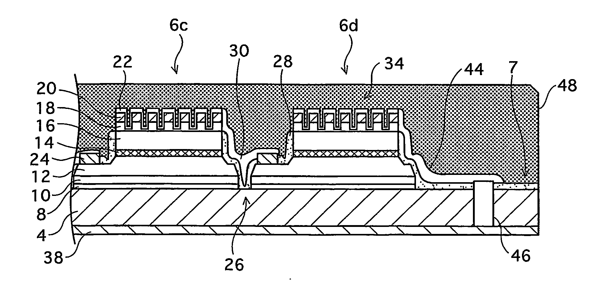
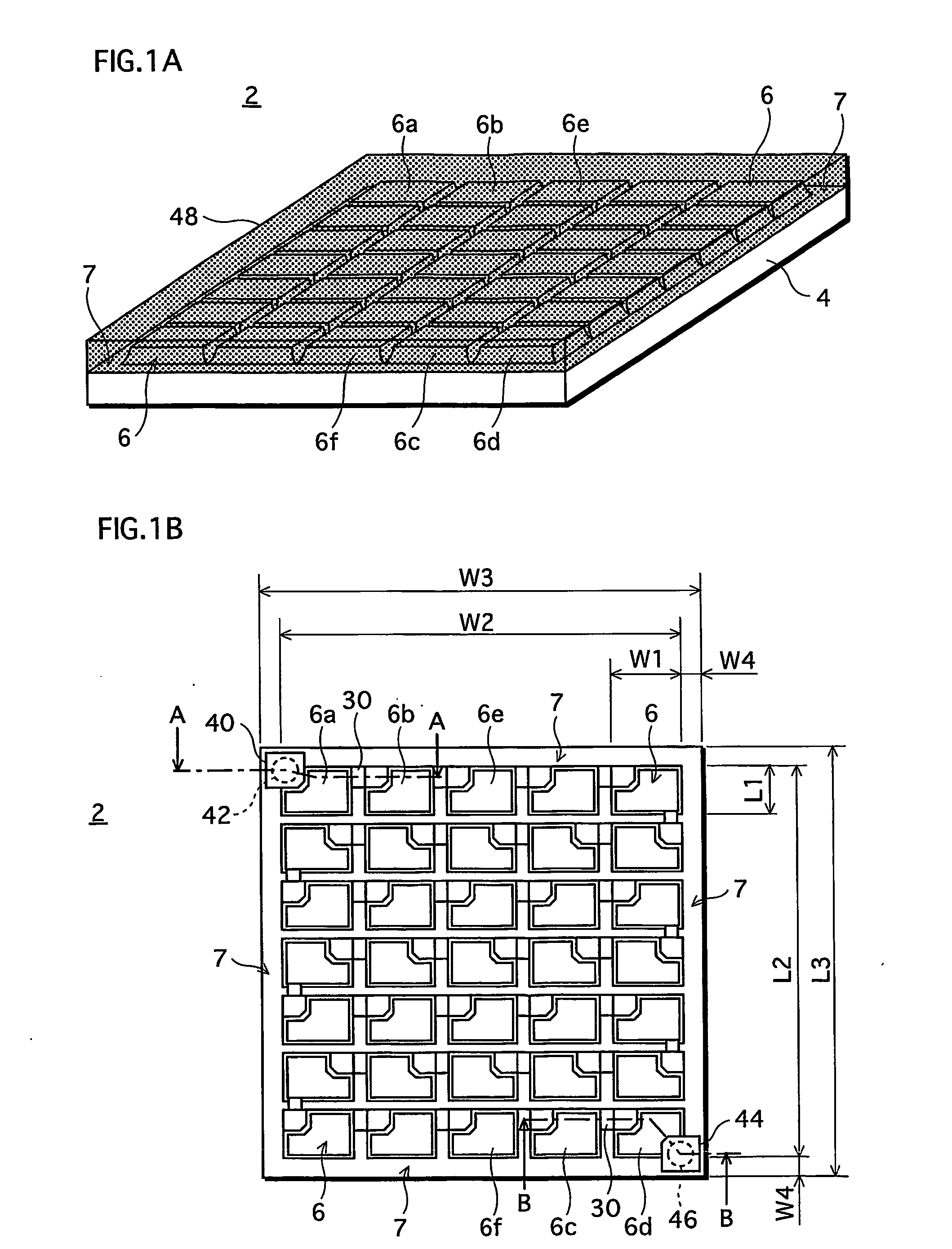
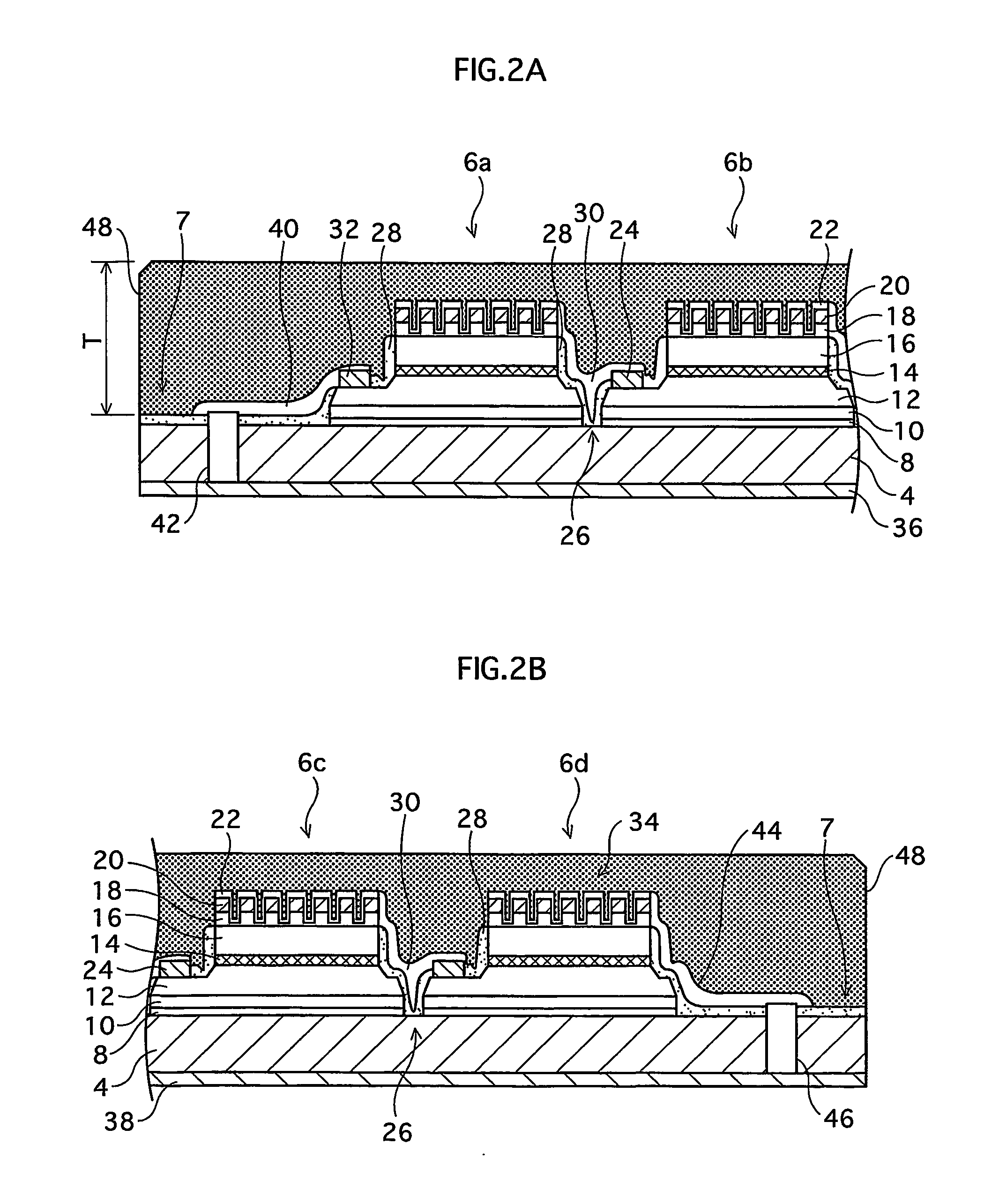
[0077]FIG. 1A is an external perspective view illustrating a construction of an LED array chip 2, which is one type of a semiconductor light emitting device, and FIG. 1B is a plan view illustrating the LED array chip 2. FIG. 1A mainly illustrates how LEDs 6 (mentioned later) are arranged in the LED array chip 2, and therefore does not show minute depressions and protrusions on surfaces of the LEDs 6. FIG. 1B illustrates the LED array chip after removing a phosphor film 48 (mentioned later).

[0078] As shown in FIGS. 1A and 1B, the LED array chip 2 is formed in such a manner that the LEDs 6 are arranged in a matrix of N rows and M columns (in the first embodiment, a matrix of seven rows and five columns, in total, 35 LEDs 6) on a non-doped (highly resistive) SiC substrate 4 which is a semiconductor substrate (hereinafter simply referred to as “an SiC substrate 4”). The LEDs 6 are light emitting elements each of which is formed by a multilayer epitaxial structure including a light emit...

first modification example of second embodiment

[0144]FIG. 14A is a plan view illustrating a white LED chip 2002 which is one type of a semiconductor light emitting device (hereinafter simply referred to as “an LED chip 2002”), FIG. 14B illustrates a cross-section of the LED chip 2002 along a line FF shown in FIG. 14A, and FIG. 14C is a bottom plan view illustrating the LED chip 2002. Here, FIG. 14A illustrates the LED chip 2002 after removing a phosphor film 2008 (shown in FIG. 14B and mentioned later). It should be noted that a reduced scale for each constituent is not uniform in any of the drawings including FIGS. 14A, 14B and 14C.

[0145] As shown in FIG. 14B, the LED chip 2002 is formed in such a manner that a multilayer epitaxial structure 2006 and the phosphor film 2008 are formed on a high-resistive Si substrate 2004 which is a base substrate (hereinafter referred to as “an Si substrate 2004”). A main surface of the Si substrate 2004 is slightly larger than a main surface of the multilayer epitaxial structure 2006. The mul...

second modification example of second embodiment

[0182] According to the first modification example of the second embodiment, the anode and cathode power supply terminals 2030 and 2032 are formed on the back main surface of the Si substrate 2004, which is a base substrate, in the LED chip 2002. In a white LED chip 2102 relating to a second modification example of the second embodiment, however, one power supply terminal (an anode power supply terminal in the second modification example) is formed on a back main surface of a base substrate, and the other power supply terminal (a cathode power supply terminal in the second modification example) is formed on a front main surface of the base substrate.

[0183] The LED chip 2102 is the same as the LED chip 2002, in terms of a composition and a thickness of each of layers constituting a multilayer epitaxial structure, and a composition of a phosphor film. However, the LED chip 2102 is different from the LED chip 2002 in terms of a construction of electrodes formed on both main surfaces o...


PUM


Abstract

An LED array chip (2), which is one type of a semiconductor light emitting device, includes an array of LEDs (6), a base substrate (4) supporting the array of the LEDs (6), and a phosphor film (48). The array of LEDs (6) is formed by dividing a multilayer epitaxial structure including a light emitting layer into a plurality of portions. The phosphor film (48) covers an upper surface of the array of the LEDs (6) and a part of every side surface of the array of LEDs (6). Here, the part extends from the upper surface to the light emitting layer.

Description

TECHNICAL FIELD [0001] The present invention relates to a semiconductor light emitting device such as a light emitting diode chip (LED chip), and also to a light emitting module, a lighting apparatus and a display element using the semiconductor light emitting device, and a manufacturing method of the semiconductor light emitting device. The present invention particularly relates to a semiconductor light emitting device that emits light of a desired color using a phosphor. BACKGROUND ART [0002] LEDs have a higher efficiency and a longer lifetime than incandescent lamps and halogen lamps. In the field of LEDs, vigorous researches have recently been conducted to use white LEDs for lighting, as white LEDs with higher luminance have been developed. A common white LED at present includes a combination of an LED bare chip emitting blue light and a phosphor excited by the blue light to emit yellow light, so that the blue light and the yellow light mix together to generate white light. [000...

Claims


Application Information

Patent Timeline
IPC IPC(8): H01L33/00F21K99/00H01L27/15H01L33/10H01L33/38H01L33/50
CPCF21K9/00H01L27/156H01L2924/12041H01L33/10H01L33/382H01L33/50H01L2933/0016H01L2933/0083H01L33/20H01L33/38H01L33/387H01L33/505H01L33/62H01L24/18H01L2924/00H01L2924/01322H01L2924/15787H01L2924/12042H01L2224/32225H01L2224/73267H01L2224/82005H01L2224/92244H01L21/568H01L24/24H01L24/82
Inventor NAGAI, HIDEO
Owner SATCO PRODS
Why Eureka
Try Eureka