Semiconductor device and manufacturing method thereof

a technology of semiconductor devices and semiconductors, applied in semiconductor devices, radio frequency controlled devices, electrical apparatus, etc., can solve the problems of insufficient low sheet resistance in inability to obtain low-resistance polymetal gate electrodes, etc., to reduce the electric resistance of the p-type polymetal gate electrode (the second gate electrode), and suppress the increase in the resistance of the gate electrode.

Inactive Publication Date: 2006-12-21
SEMICON PATENT
View PDF2 Cites 14 Cited by
  • Summary
  • Abstract
  • Description
  • Claims
  • Application Information

AI Technical Summary

Benefits of technology

[0009] The present invention has been achieved to solve the above problems. It is an object of the present invention to provide a semiconductor device and a manufacturing method thereof that can prevent mutual diffusion of impurity in a silicide layer and can decrease sheet resistance of an N-type polymetal gate electrode and a P-type polymetal gate electrode, respectively in the semiconductor device having gate electrodes of a polymetal gate structure and a dual gate structure.
[0012] According to the present invention, the silicide layer is set discontinuous on the P-type silicon layer, thereby suppressing the increase in the resistance of the gate electrode due to mutual diffusion of impurity. At the same time, the surface of the silicide layer discontinuous from the surface of the P-type silicon layer exposed to the discontinuous part of the silicide layer is continuously covered with a silicon film. With this arrangement, the sheet resistance of the P-type polymetal gate electrode (the second gate electrode) can be decreased.
[0013] A non-doped silicon film is preferably used for the first and the second silicon films. With this arrangement, it becomes possible to further decrease the electric resistance of the P-type polymetal gate electrode. This is considered due to the following reason. When the metal nitride layer is in contact with the silicon layer containing much P-type impurity, the reaction between the metal nitride layer and the silicon layer is promoted due to the P-type impurity contained in the silicon layer. As a result, a thick metal silicide nitride layer is formed. On the other hand, the non-doped silicon film has small reaction with the metal nitride layer. Therefore, even when a metal silicide nitride film is formed, this film thickness can be decreased.

Problems solved by technology

When the metal silicide nitride layer has a large film thickness, a low-resistance polymetal gate electrode cannot be obtained.
However, as described in Japanese Patent Application Laid-Open No. 2003-163348, when an electrode of a polymetal gate structure having a lamination of a polysilicon layer, a silicide layer, a metal nitride layer, and a metal layer is applied to the dual gate structure, the following problem occurs.
However, it has become clear that when the silicide layer is formed discontinuously on the P-type polysilicon layer, sufficiently low sheet resistance cannot be obtained in the P-type polymetal gate electrode, in some cases.

Method used


Image

  • Semiconductor device and manufacturing method thereof
  • Semiconductor device and manufacturing method thereof
  • Semiconductor device and manufacturing method thereof

Examples


Embodiment Construction

[0029] Preferred embodiments of the present invention will be explained below with reference to the accompanying drawings.

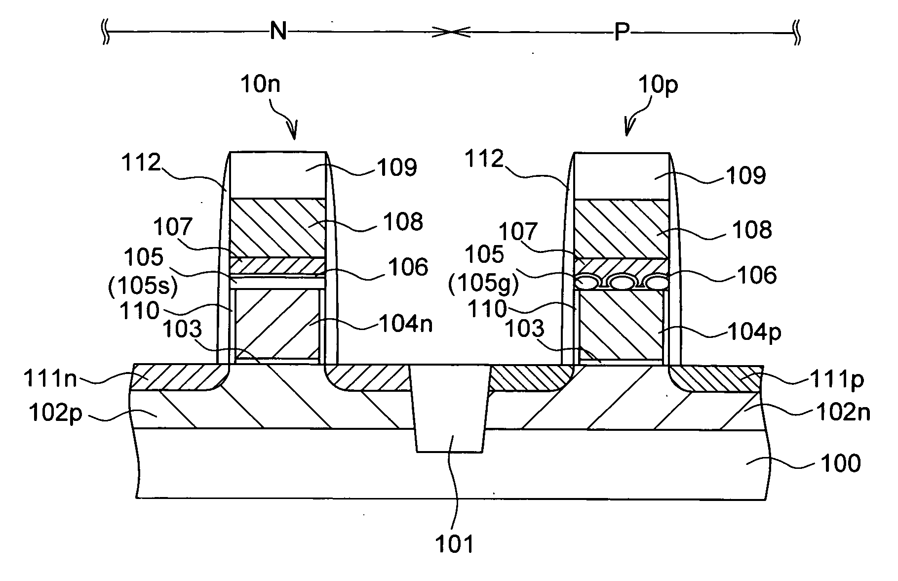
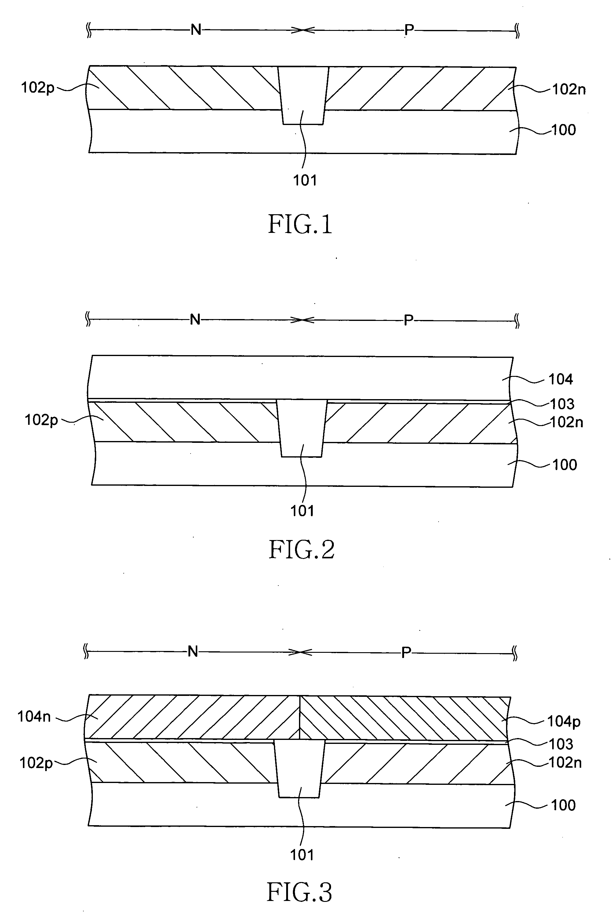
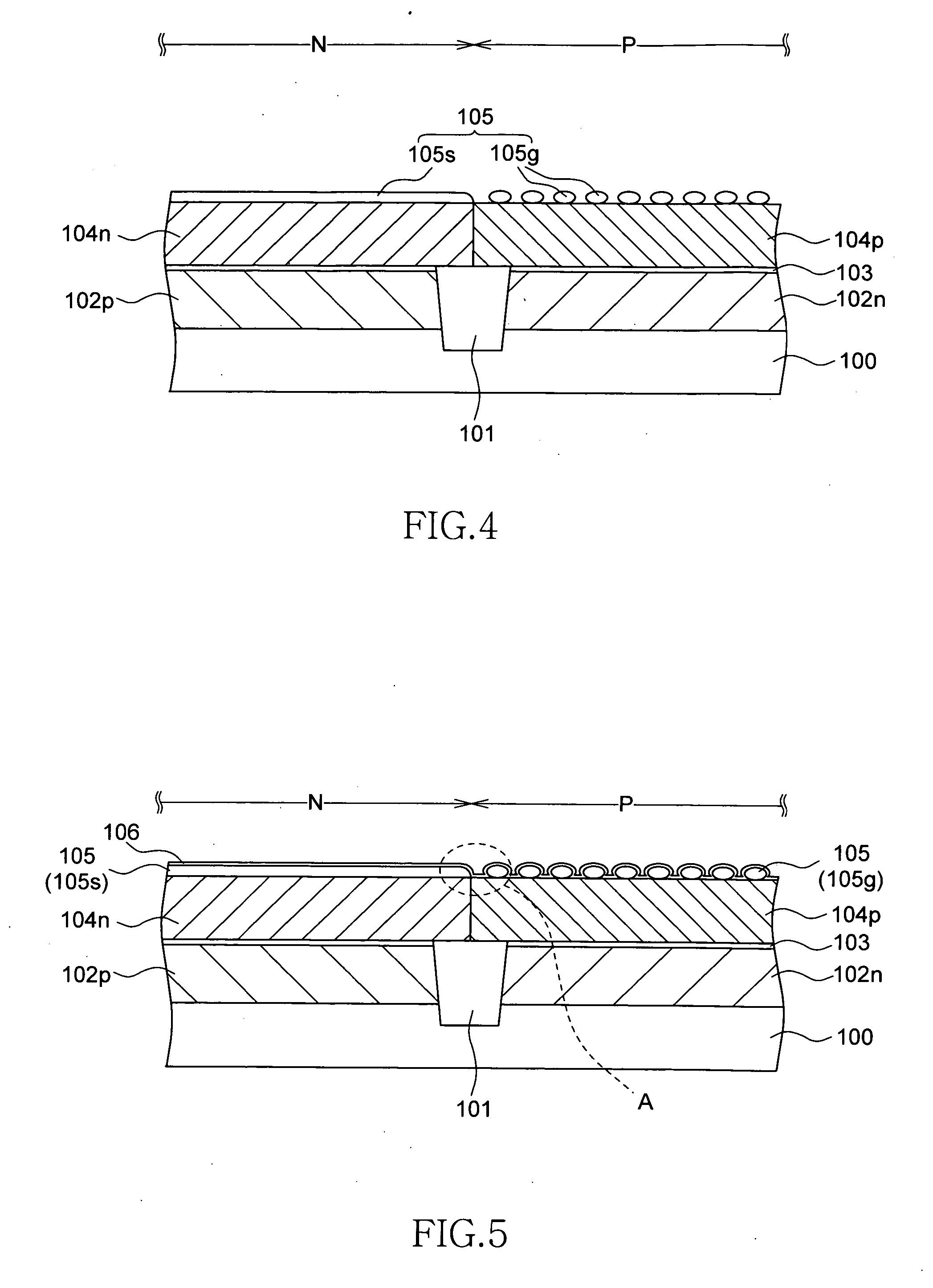
[0030]FIG. 1 to FIG. 10 are process diagrams schematically showing a process of manufacturing an N-channel transistor and a P-channel transistor having gate electrodes of polymetal gate and dual gate structures according to an embodiment of the present invention. In FIG. 1 to FIG. 10, a “region N” denotes a region in which an N-channel transistor including an N-type polymetal gate electrode is formed, and a “region P” denotes a region in which a P-channel transistor including a P-type polymetal gate electrode is formed.

[0031] First, as shown in FIG. 1, an element isolation insulation film 101 is formed in a predetermined region of a semiconductor substrate 100, according to a shallow trench isolation (STI) technique, thereby isolating the region N from the region P. Next, boron (B) is doped as P-type impurity in the region N, thereby forming a P well 102p, and ...


PUM


Abstract

A semiconductor device and a manufacturing method thereof that can prevent mutual diffusion of impurity in a silicide layer and can decrease sheet resistance of an N-type polymetal gate electrode and a P-type polymetal gate electrode, respectively in the semiconductor device having gate electrodes of a polymetal gate structure and a dual gate structure are provided. The P-type polymetal gate electrode includes a P-type silicon layer containing P-type impurity, a silicide layer formed on the P-type silicon layer and having a plurality of silicide grains which are discontinuously disposed in a direction substantially parallel with the surface of the semiconductor substrate, a silicon film continuously formed on the surface of the P-type silicon layer exposed on the discontinuous part of the silicide layer and on the surface of the silicide layer, a second metal nitride layer formed on the silicon film, and a metal layer formed on the metal nitride layer.

Description

TECHNICAL FIELD [0001] The present invention relates to a semiconductor device and a manufacturing method thereof. Particularly, the invention relates to a semiconductor device having gate electrodes of a polymetal gate structure and a dual gate structure, and a manufacturing method of this semiconductor device. BACKGROUND OF THE INVENTION [0002] Recently, a polymetal gate structure of a semiconductor device, particularly, a DRAM (Dynamic Random Access memory) has been widely used, in order to improve the operation speed of the device. [0003] The polymetal gate structure is a gate electrode structure having a metal layer laminated on a polysilicon layer. The polymetal gate structure is known to decrease resistance (sheet resistance) of a word line in a plane direction more than a polycide gate structure that is used conventionally. However, when a metal layer (for example, tungsten (W)) is directly formed on the polysilicon layer, the polysilicon layer reacts with the metal layer in...

Claims


Application Information

Patent Timeline
Patent Type & Authority Applications(United States)
IPC IPC(8): H01L29/76
CPCH01L21/28061H01L21/823835H01L29/78H01L29/4933H01L21/823842H01L21/28518H01L29/665
Inventor TAGUWA, TETSUYA
Owner SEMICON PATENT
Why Eureka
Try Eureka