

High-mobility MOS (Metal Oxide Semiconductor) capacitor and manufacturing method thereof
A high-mobility, production method technology, applied in the field of high-mobility MOS capacitors and its production, can solve the problems of imperfect interfaces, high interface state density, and electron mobility not reaching the expected goal, so as to improve electrical performance, Effects of prevention of interdiffusion, reduction of defect charge and interface state density
- Summary
- Abstract
- Description
- Claims
- Application Information
AI Technical Summary
Problems solved by technology
Method used
Image

Examples
Embodiment Construction
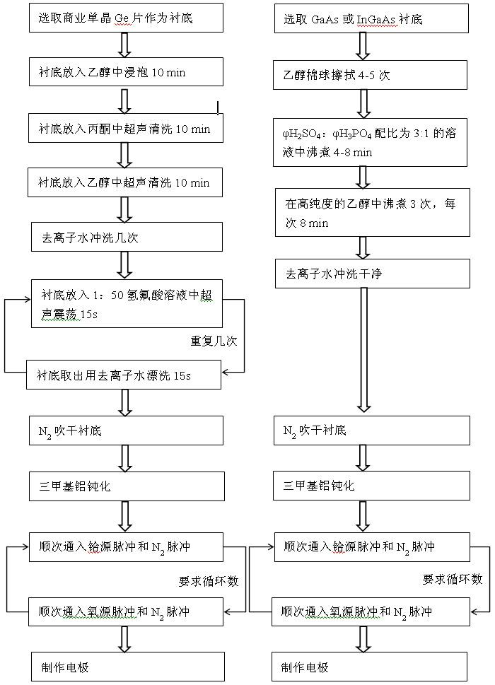
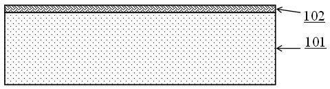
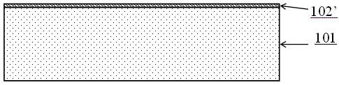
[0025] The present invention will be further described in detail below in conjunction with the fabrication flow chart of the entire high-mobility MOS capacitor and specific implementation methods. In the drawings, the thicknesses of layers and regions are enlarged or reduced for convenience of description, and the shown sizes do not represent actual sizes. Although these figures do not fully reflect the actual size of the device, they still fully reflect the interrelationships between the regions and the constituent structures.
[0026] 1) If the substrate is a germanium (Ge)-based substrate, the steps are as follows:
[0027] Step 1: Select a commercial single crystal Ge wafer, n-type Sb doped, crystal orientation (100), resistivity 0.21-0.26 Ω·cm as the substrate, namely figure 2 101 layer in , but there will be a layer of naturally oxidized GeO on the surface of Ge substrate without cleaning x ,Right now figure 2 102 floors in;
[0028] Step 2: Soak the substrate in ...
PUM
 Abstract
Description
Claims
Application Information