Film system structure of moderate and high temperature solar energy selective absorption coating and production method thereof
A film structure and selective technology, applied in the direction of solar thermal power generation, solar thermal devices, coatings, etc., can solve the problem that the surface anti-reflection layer is not strong in anti-atmospheric environment, the preparation equipment and process are complex, and it is not suitable for large-scale industrial production and other issues, to achieve high light-to-heat conversion efficiency, maintain light performance, and improve anti-reflection effects
- Summary
- Abstract
- Description
- Claims
- Application Information
AI Technical Summary
Problems solved by technology
Method used
Image
Examples
Embodiment 1
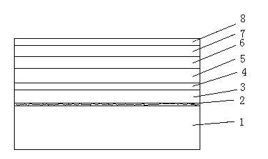
[0048] Embodiment 1, as attached figure 1 shown
[0049] A film structure of a medium-high temperature solar selective absorption coating, including a substrate 1, an ion-etched layer 2 integrated with the substrate 1 on one surface of the substrate 1, and an ion-etched layer 2 formed on the surface of the ion-etched layer 2 from the inside There are aluminum infrared reflective film layer 3, titanium nitride thermal diffusion barrier film layer 4, high metal content titanium oxynitride selective absorption film layer 5, low metal content titanium oxynitride selective absorption film layer 6, tetranitrogen Silicon trisilicon anti-reflection film layer 7, and silicon dioxide anti-reflection film layer 8.
[0050] The substrate 1 is a stainless steel or copper or aluminum metal substrate, or a glass substrate.
[0051] The thickness of the aluminum infrared reflective film layer 3 is in the range of 85-95 nm, the thickness of the titanium nitride thermal diffusion barrier film...
Embodiment 2
[0052] Example 2, see attached figure 1
[0053] A method for preparing a film structure of a medium-high temperature solar selective absorption coating, using a metal copper substrate 1 as a starting material, and using a vacuum magnetron sputtering coating machine as a processing device, the preparation method is as follows;
[0054] 1. Pretreatment of metal copper substrate 1
[0055] The copper foil substrate 1 is ultrasonically cleaned in an alkaline solution, rinsed with clean water, put into a weakly acidic solution for neutralization, and then undergoes chemical treatment to form a certain roughness on the surface of the substrate 1, increase the specific surface area of the substrate 1, reduce The reflection of light can obtain a certain degree of structural "light trapping" and improve the absorptivity of the coating. Then the substrate 1 was dried and placed in a coating vacuum chamber to keep warm for 10 minutes at a temperature of 200°C. The background vacuum...
PUM
| Property | Measurement | Unit |
|---|---|---|
| thickness | aaaaa | aaaaa |
| thickness | aaaaa | aaaaa |
| thickness | aaaaa | aaaaa |
Abstract
Description
Claims
Application Information
