Electronic devices and a method for encapsulating electronic devices
a technology of electronic devices and encapsulation methods, which is applied in the manufacture of electrode systems, electric discharge tubes/lamps, and discharge tubes luminescnet screens, etc., can solve the problems of low work function metals, low device thickness, and decreased performance of organic electronic devices, so as to reduce process time and cost, simplify the encapsulation process, and reduce the thickness of the device
- Summary
- Abstract
- Description
- Claims
- Application Information
AI Technical Summary
Benefits of technology
Problems solved by technology
Method used
Image
Examples
example 1
[0107] This example illustrates the present invention applying the getter composition. The getter composition was a liquid dispersion of particles of a zeolite-based molecular sieve and glass frit in an organic liquid medium. The dispersion comprised the following ingredients by wt % of total dispersion:
Inorganic components:Zeolite-based molecular sieve (13x-typed powder)54.1Glass frit5.4Organic components:surfactant1.1ethylcellulose resin1.0Texanol solvent (ester alcohol)38.4%
[0108] The composition of the glass frit in wt % (dry) was as follows:
SiO2Al2O3B2O3CaOZnOBi2O37.112.138.380.5312.0369.82
example 2
[0109] This example illustrates making and performance of method of applying the getter composition of the present invention. A slurry of 0.75 tablets of unfired DESIWAFER 300 / 20 zeolite-clay material in 1 ml of water was dispersed in water to make a 200 ml dispersion. The dispersion was applied to a cavity on a glass lid plate in 0.5 ml aliquots by hand using a syringe. The getter was solidified by placing in a vacuum oven for 1 hour at 70° C. to remove substantially all of the water. After solidification, the getter layers were then activated and densified by heating the glass lid plates for 2 hours at 500° C. In an environment having less than 10 ppm H2O and O2, the plates with self-attached getter layers were then each assembled into an enclosure holding a polymer light emitting diode device (“PLED”). Control devices were assembled into an enclosure under the same conditions, except that the getter layer was replaced by a fired DESIWAFER tablet (Sud-Chemie) attached to a plate b...
example 3
[0110] This example illustrates the use of a sealing composition comprising spacer beads dispersed in epoxy to provide the separation between two flat plates in an organic electronic device. This example further illustrates the use of a getter ledge for sealing under reduced pressure.
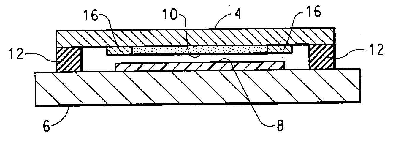
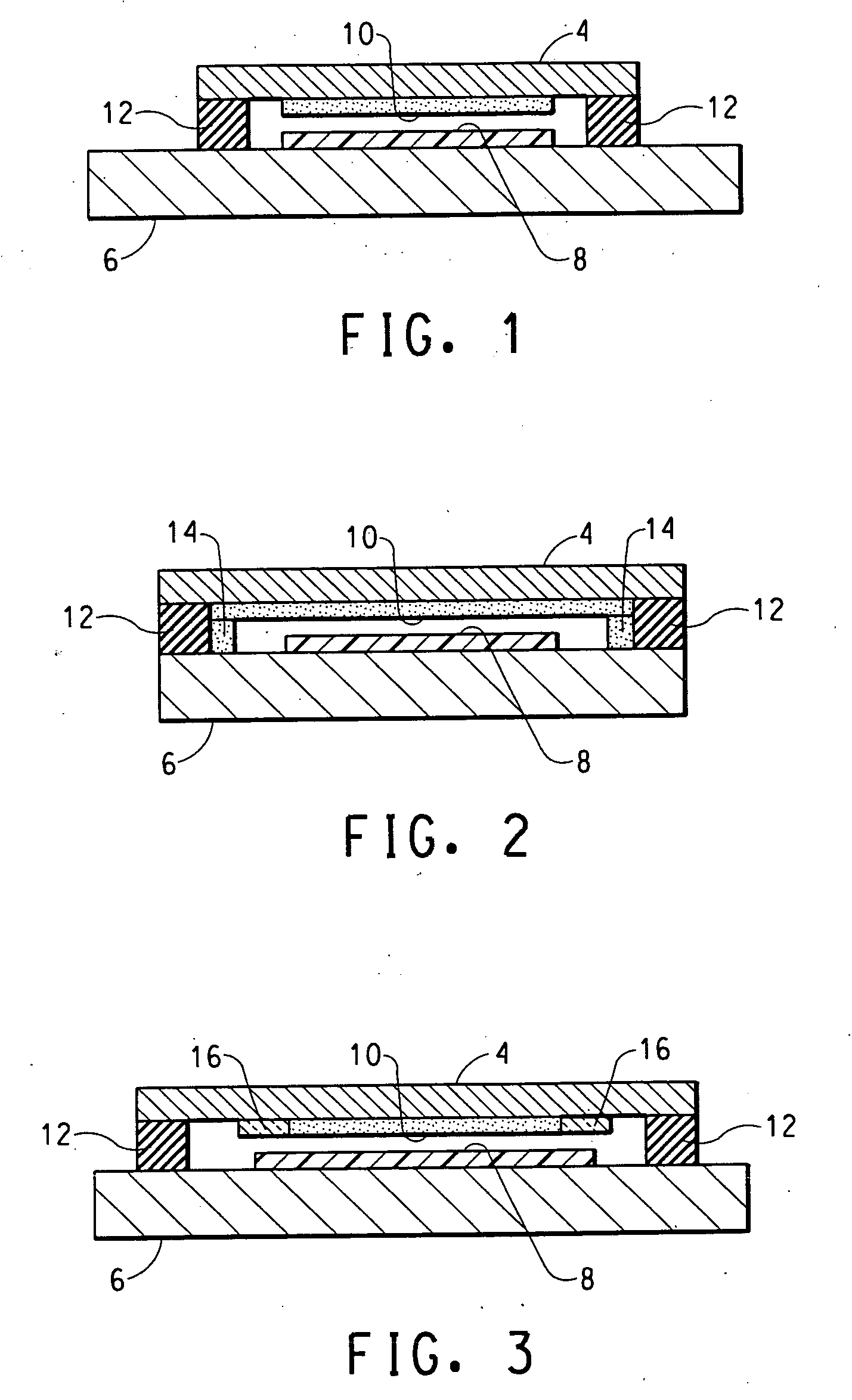
[0111] An approximately 30 micron getter layer was formed on an approximately 0.3 mm thickness flat glass lid using the method as described in Example 2. The getter layer was formed in a pattern to provide a ledge around the perimeter of a device. An OLED was formed on an approximately 0.3 mm thickness flat glass substrate, and an epoxy containing 2% by volume of 50 micron glass frit beads was used to seal the lid to the OLED. The epoxy was applied to the exterior of the getter ledge and the device was sealed under vacuum. The resulting device had a thickness of approximately 0.64 mm.
[0112] Note that not all of the activities described above in the general description or the examples are required, tha...
PUM
| Property | Measurement | Unit |
|---|---|---|
| diameter | aaaaa | aaaaa |
| diameter | aaaaa | aaaaa |
| absolute pressure | aaaaa | aaaaa |
Abstract
Description
Claims
Application Information


