
Silane monomers and siloxane polymers for semiconductor optoelectronics

a technology of semiconductor optoelectronics and monomers, which is applied in the direction of plastic/resin/waxes insulators, organic insulators, coatings, etc., can solve the problems of low thermal stability, the organic polymer cannot be chemically mechanically polished or etched back by dry processing without damaging the film, etc., to achieve excellent chemical resistance, low chemical adsorption behavior, and high cross-linking

Inactive Publication Date: 2006-12-28
SILECS OY
View PDF4 Cites 11 Cited by
  • Summary
  • Abstract
  • Description
  • Claims
  • Application Information

AI Technical Summary

Benefits of technology

[0013] It is a third object of the invention to provide methods of producing poly(organo siloxane) compositions, which are suitable for the preparation of thin films having excellent dielectric properties and optical properties.
[0034] Furthermore, the novel materials have excellent gap fill properties.

Problems solved by technology

However, applicability of these films is limited because of their low thermal stability, softness, and incompatibility with traditional technological processes developed for SiO2 based dielectrics.
For example, organic polymer cannot be chemical mechanical polished or etched back by dry processing without damaging the film.
However, these organic units reduce the degrees of bridging crosslinks as well increases the free volume between the molecules due to steric hindrance.

Method used


Image

  • Silane monomers and siloxane polymers for semiconductor optoelectronics
  • Silane monomers and siloxane polymers for semiconductor optoelectronics
  • Silane monomers and siloxane polymers for semiconductor optoelectronics

Examples


example 1

1,1,1,4,4-Pentachloro-1,4-disilabutane (The Intermediate)

[0097]

[0098] Vinyltrichlorosilane (68.8 g, 426 mmol) and cobalt octacarbonyl (700 mg) were placed in a 100 mL rb flask and cooled in an ice bath to 0 ° C. Dichlorosilane (bp. 8 ° C., 44.3 g, 439 mmol) was then condensed into the flask, The system was allowed to warm up to room temperature during night. Distillation at 60 . . . 62° C. / 8 mbar gave 1,1,1,4,4-Pentachloro-1,4-disilabutane (120.8 g, 460 mmol) in 93% yield.

example 2

Tris(3,3,6,6,6-pentachloro -3,6-disilahexyl)chlorosilane

[0099]

[0100] 11.00 g (0.076 mol) trivinylchlorosilane was added to a 100 ml vessel followed by 2 ml 1,1,1,4,4-pentachloro- 1,4-disilabutane. The solution was heated to 80° C. and 15 μL of a 10% H2PtCl6 / IPA -solution was added. Strong exothermic reaction was observed and heat was switched off. Rest of 1,1,1,4,4-pentachloro-1,4-disilabutane was added slowly during 30 min keeping the temperature of the solution below 130° C. The total amount of 1,1,1,4,4-pentachloro-1,4-disilabutane was 61.50 g (0.234 mol, 2.6% excess). After addition heat was again switched on and solution was stirred for an hour at 110° C. After that solution was distilled yielding 47.08 g (66%) tris(3,3,6,6,6-pentachloro-3,6-disilahexyl)chlorosilane. B.p. 264° C. / <0.5 mbar.

example 3

1,1,1,4,4,7,7,7-Octachloro-1,4,7-trisilaheptane

[0101]

[0102] Vinyltrichlorosilane (16.8 g, 104 mmol) was heated to 60° C. and 100 μL 10% H2PtCl6 / IPA-solution was added. 1,1,1,4,4-pentachloro- 1,4-disilabutane (20.4 g, 77.7 mmol) was added slowly during 20 min so that the temperature did not exceed 100° C. The reaction was allowed to proceed for 12 hours at 100° C., after which it was distilled under vacuum at 115-130° C. / <1 mbar. The yield was 31.5 g (74.3 mmol, 96%).


PUM

PropertyMeasurementUnit
thicknessaaaaaaaaaa
thicknessaaaaaaaaaa
thicknessaaaaaaaaaa

Abstract

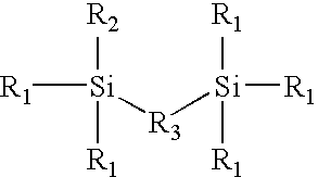
A method for producing a polymer for semiconductor optoelectronics, comprising the steps of providing a monomer is produced having the formula: wherein: R1 is a hydrolysable group R2 is hydrogen, and R3 is a bridging linear or branched bivalent hydrocarbyl group, said monomer being produced by hydrosilylation of the corresponding starting materials, and homo- or copolymerizing the monomer to produce a polymer.

Description

[0001] This application claims priority of U.S. Provisional Application for Patent Ser. No. 60 / 689,541 filed Jun. 13, 2005, which is incorporated herein by reference.BACKGROUND OF THE INVENTION [0002] 1. Field of the Invention [0003] The present invention relates to a method making novel organo fuictionalized silane precursors and polymers of the same that are applicable for thin films used for example as dielectrics in integrated circuits, optoelectronic applications and for other similar applications. In particular, the invention concerns first making an intermediate monomer and then converting the monomer to an organo functionalized silane monomer and finally forming a polymer or polymer compositions of the functionalized monomers. The invention also concerns a method for producing such films by preparing siloxane compositions by polymerization of the organo functionalized monomers, by applying the polymerized compositions on a substrate in the form of a layer and by curing the l...

Claims


Application Information

Patent Timeline
Patent Type & Authority Applications(United States)
IPC IPC(8): C08G77/04C08G77/08C08L83/04
CPCC08G77/08C08G77/50C09D183/04C09D183/14H01L21/3127H01L21/02126H01L21/02216H01L21/02282H01L21/3122H01B3/46Y10T428/31663H01L21/0212
Inventor RANTALA, JUHA T.PAULASAARI, JYRIPIETIKAINEN, JARKKO
Owner SILECS OY
Learn More