Semiconductor device having a recess gate for improved reliability

a technology of semiconductor devices and recesses, which is applied in the direction of semiconductor devices, basic electric elements, electrical appliances, etc., can solve the problems of difficult to sufficiently enlarge the step difference between the channel area and the source/drain area, increase the amount of ions implanted into the source/drain area, and increase the resistance of parasitic series and spiking phenomenon, so as to reduce the parasitic series resistance and spiking phenomenon

Active Publication Date: 2007-01-04
SK HYNIX INC
View PDF6 Cites 15 Cited by
  • Summary
  • Abstract
  • Description
  • Claims
  • Application Information

AI Technical Summary

Benefits of technology

[0022] Accordingly, the present invention has been made to solve the above-mentioned problems occurring in the prior art, and an object of the present invention is to provide a method...

Problems solved by technology

Due to the short channel effect, a threshold voltage (Vt) is significantly lowered and a drain induced barrier lowering (DIBL) effect is generated, causing problems when the semiconductor devices are operated.
In addition, with increasing degree of high integration in a semiconductor device, more ions are excessively implanted into the source/drain area, and the depth of the source/drain area becomes shallow.
Thus, it is difficult to sufficiently enlarge the step difference size between the channel area and the source/drain area by utilizing the conventional recess gate forming techniques.
Therefore, there are limitations to reduce the parasitic series resistance and spiking phenomenon.
In addition, when the oxide layer 4 is grown through the LOCOS process, an unwanted deposition resembling a bird's beak (not shown) is formed at each of the end portions of the oxide layer, so there is limitation to reduce the line width of the gate.
Accordingly, an RC delay may occur in the semiconductor device fabricate...

Method used


Image

  • Semiconductor device having a recess gate for improved reliability
  • Semiconductor device having a recess gate for improved reliability
  • Semiconductor device having a recess gate for improved reliability

Examples


Embodiment Construction

[0042]FIGS. 3A to 3G are cross-sectional views for illustrating the procedure for manufacturing a semiconductor device according to one embodiment of the present invention.

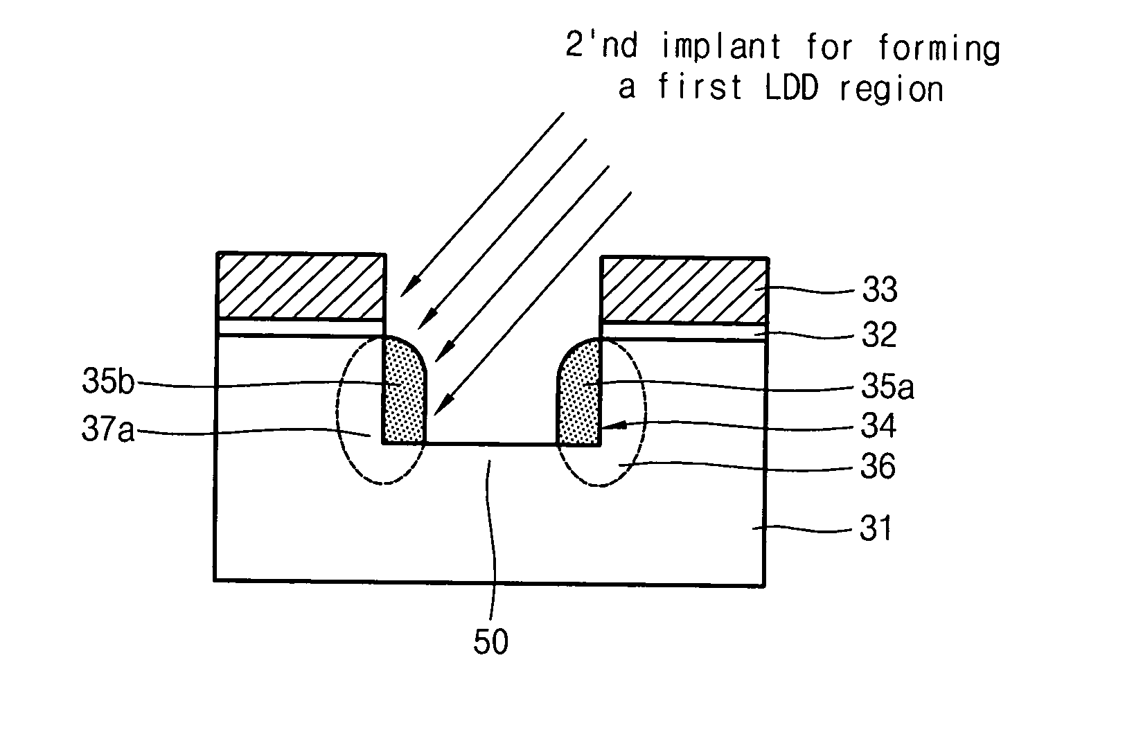
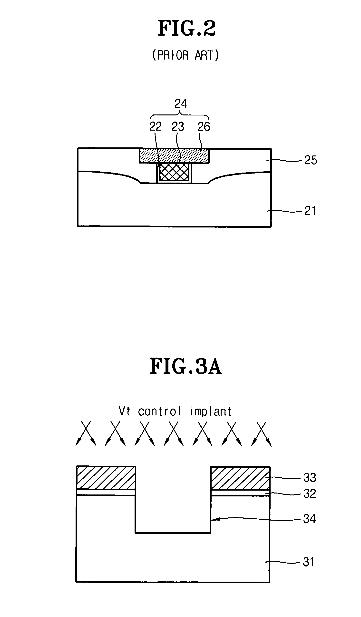
[0043] Referring to FIG. 3A, a pad oxide layer 32 having a thickness of about 50 to 100 Å is formed on a semiconductor substrate 31, and a pad nitride layer 33 having a thickness above 1500 Å is formed on the pad oxide layer 32. Then, the pad nitride layer 33 and the pad oxide layer 32 are etched, thereby exposing a gate area of the semiconductor substrate 31. After that, the exposed portion of the semiconductor substrate 31 is etched by a thickness of about 500 to 1000 Å by using the etched pad nitride layer 33 as an etching barrier, thereby forming a recess 34.

[0044] Then, a threshold voltage (Vt) control implantation process is performed with respect to the resultant substrate having the recess 34 at the gate area, to increase the boron concentration on the sidewall of the recess channel. For example, the thr...


PUM


Abstract

A semiconductor device having a recess gate is formed by first forming a recess below the upper surface of the substrate. A spacer is formed at each sidewall of the recess. An impurity doping area is formed in a source area. A first LDD area is formed in a drain area. A gate comprising a gate insulating layer and a gate conductive layer is then formed in the recess. A second LDD area is formed on the upper surface of the semiconductor substrate. A gate spacer is formed at each sidewall of the gate. Then a source/drain area having an asymmetrical structure is formed on each side of the gate.

Description

BACKGROUND OF THE INVENTION [0001] 1. Field of the Invention [0002] The present invention relates generally to a method of manufacturing a semiconductor device. More particularly, the present invention relates to a method of manufacturing a semiconductor device having a recess gate for improving reliability of the semiconductor device. [0003] 2. Description of the Prior Art [0004] In general, as semiconductor devices are highly integrated, the gate channel lengths of the highly integrated semiconductor devices are significantly shortened. For this reason, the charge-sharing phenomenon frequently occurs between the source and drain areas of a gate (collectively referred to as the “source / drain area”) contributing to degradation of the gate control function—this is known as a “short channel effect”. Due to the short channel effect, a threshold voltage (Vt) is significantly lowered and a drain induced barrier lowering (DIBL) effect is generated, causing problems when the semiconductor ...

Claims


Application Information

Patent Timeline
IPC IPC(8): H01L21/8242H01L21/8222
CPCH01L21/26586H01L29/1083H01L29/7834H01L29/66553H01L29/66621H01L29/4983H01L21/18
Inventor JANG, MIN WOO
Owner SK HYNIX INC
Why Eureka
Try Eureka