Supercharge Your Innovation With Domain-Expert AI Agents!

Silicon wafer support fixture with roughended surface

a technology of support fixture and silicon wafer, which is applied in the direction of crystal growth process, polycrystalline material growth, chemically reactive gas, etc., can solve the problems of reducing the yield of operable integrated circuit dies obtained from the wafer, thermal cvd tends to coat all surfaces exposed in the furnace, and significant problems with particle production, so as to achieve convenient formation

Inactive Publication Date: 2007-01-11
ZEHAVI RANAAN Y +1
View PDF37 Cites 6 Cited by
  • Summary
  • Abstract
  • Description
  • Claims
  • Application Information

AI Technical Summary

Problems solved by technology

However, thermal CVD tends to coat all surfaces exposed in the furnace.
However, as the feature sizes on integrated circuits has decreased to 0.18 μm and even smaller, quartz support towers have nonetheless experienced substantial problems with producing particles.
These particulates fall on the wafer and can significantly reduce the yield of operable integrated circuit dies obtained from the wafer.
However, after some number of runs, the number of particles greatly increases to a totally unacceptable level.
It is believed that the origin of the problem is that the silicon nitride is also depositing on the quartz tower.
Although quartz towers are relatively inexpensive, such short life greatly increases the cost of ownership (COO) when measured per wafer.
Also, the necessity of changing out towers and cleaning towers complicates the work flow and reduces productivity.
Both factors reduce the yield of operable dice obtained from the wafers.
However, the CVD silicon carbide film is fragile, and a single pin hole through the film ruins the coating protect so the tower must be scrapped.
Entire towers of CVD silicon carbide can be made, but they are very expensive.

Method used


Image

  • Silicon wafer support fixture with roughended surface
  • Silicon wafer support fixture with roughended surface
  • Silicon wafer support fixture with roughended surface

Examples


Embodiment Construction

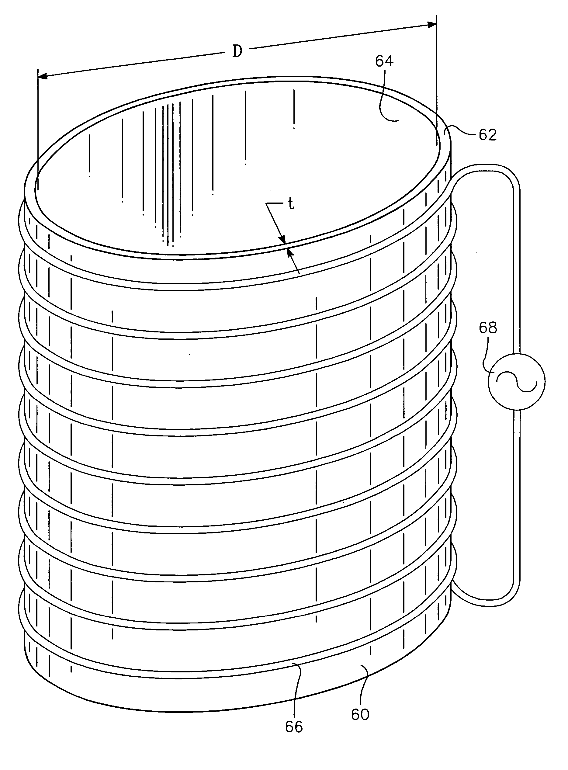
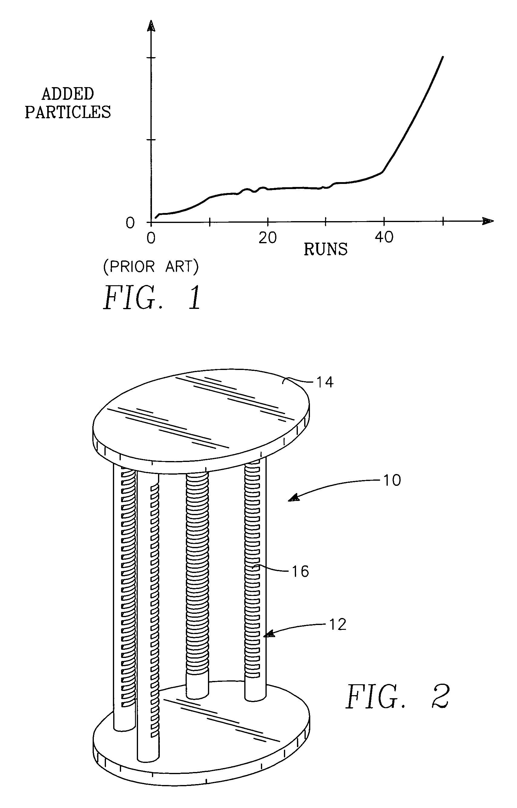
[0026] Silicon fixtures, particularly horizontally extending boats, have been frequently suggested and occasionally used in the past. However, their assembly has presented sufficient problems to prevent the widespread use of silicon towers. Many of these problems with silicon support fixtures have been addressed in a set of patents, U.S. Pat. Nos. 6,196,211, 6,205,993, and 6,225,594 to various of Zehavi, Davis, and Delaney. Boyle et al. in U.S. patent application, Ser. No. 09 / 608,291, filed Jun. 30, 2000, now issued as U.S. Pat. No. 6,455,395, and incorporated herein by reference in its entirety, disclose in detail a method of fabricating one embodiment of such a silicon tower 10, illustrated in FIG. 2. The tower 10 includes multiple silicon legs 12 joined at opposed ends to silicon bases 14. Teeth 16 are cut into the legs 12 to support the wafers.

[0027] It is preferred that at least the legs 12 are composed of virgin polysilicon (virgin poly) formed from the chemical vapor deposit...


PUM

PropertyMeasurementUnit
temperaturesaaaaaaaaaa
roughnessaaaaaaaaaa
roughnessaaaaaaaaaa

Abstract

A silicon-based wafer support tower particularly useful for batch-mode thermal chemical vapor deposition. The surfaces of the silicon tower are bead blasted to introduce sub-surface damage, which produces pits and cracks in the surface, which anchor subsequently deposited layer of, for example, silicon nitride, thereby inhibiting peeling of the nitride film. The surface roughness may be in the range of 0.25 to 2.5 μm. Wafer support portions of the tower are preferably composed of virgin polysilicon. The invention can be applied to other silicon parts in a deposition or other substrate processing reactor, such as tubular sleeves and reactor walls. Tubular silicon members are advantageously formed by extrusion from a silicon melt.

Description

RELATED APPLICATION [0001] This application is a division of Ser. No. 09 / 860,392, filed May 18, 2001 and to be issued on Sep. 19, 2006 as U.S. Pat. No. 7,108,746, incorporated herein by reference.BACKGROUND OF THE INVENTION [0002] 1. Field of the Invention [0003] The invention relates generally to semiconductor processing. In particular, the invention relates to wafer support fixtures used in batch-mode chemical vapor deposition. [0004] 2. Background Art [0005] The fabrication of silicon integrated circuits typically involves one or more steps of chemical vapor deposition (CVD). Many advanced deposition processes use plasma enchanced CVD to activate the chemical reaction resulting in the deposition of the film from a precursor gas. The plasma process allows low temperature deposition. On the other hand, thermal CVD is performed at elevated temperatures to thermally activate the chemical reaction resulting in the deposition of the film from a precursor gas. The temperatures associate...

Claims


Application Information

Patent Timeline
Patent Type & Authority Applications(United States)
IPC IPC(8): C30B23/00C30B25/00C30B28/12C30B28/14C23C16/44C23C16/458C30B25/02C30B25/12C30B35/00H01L21/673
CPCC23C16/4404C23C16/4581H01L21/67306C30B25/12C30B35/00C30B25/02
Inventor ZEHAVI, RANAAN Y.BOYLE, JAMES E.
Owner ZEHAVI RANAAN Y
Features
  • R&D
  • Intellectual Property
  • Life Sciences
  • Materials
  • Tech Scout
  • Unparalleled Data Quality
  • Higher Quality Content
  • 60% Fewer Hallucinations
Learn More