Light-emitting device, method for producing same, and display

a technology of light-emitting devices and light-emitting lamps, which is applied in the direction of electroluminescent light sources, thermoelectric devices, electric lighting sources, etc., can solve the problems of low brightness, inability to actively develop inorganic light-emitting devices for practical use, and complicated driving circuits of such devices, etc., to achieve excellent in-plane uniformity of light brightness, long lifespan, and high brightness

Inactive Publication Date: 2007-01-11
PANASONIC CORP
View PDF8 Cites 71 Cited by
  • Summary
  • Abstract
  • Description
  • Claims
  • Application Information

AI Technical Summary

Benefits of technology

[0020] It is therefore an object of the present invention to provide a top emission-type light-emitting device having high brightness, excellent in-plane uniformity of luminous brightness, long lifespan, and stable light emission quality, a manufacturing method of such a light-emitting device, and a display using the light-emitting device.

Problems solved by technology

Inorganic EL devices using inorganic materials such as zinc sulfide require a relatively high alternating voltage to operate, and therefore driving circuits thereof are likely to be complicated.
In addition, such inorganic EL devices have a problem that brightness is low.
For these reasons, inorganic EL devices have not been so actively developed for practical use.
In the case of an active matrix display having thin film transistors which drive individual pixels, the thin film transistors are arranged on the transparent substrate, and therefore it is difficult for such a conventional active matrix display to have a high aperture ratio.
However, in this case, formation of an ITO film usually used as a transparent electrode involves a problem that the organic layers provided below the ITO film are deteriorated under the influence of heat applied thereto during forming the ITO film so that carrier injection does not sufficiently occur.
In general, an organic EL device is deteriorated under the influence of moisture or oxygen, thereby lowering brightness or increasing dark spots.
In a case where a thin metal film or resin film is used for a light extraction surface, the lifespan of the device is shortened because such a film is inferior in moisture and oxygen barrier properties to a glass substrate or the like.
As described above, a top emission-type light-emitting device can have a high aperture ratio, but it is difficult to achieve high brightness, high reliability, and long lifespan at the same time.
The brightness of a display using an organic EL device can be improved by increasing the current density flowing through an organic light-emitting material of the organic EL device, but the organic light-emitting material is likely to deteriorate due to an increased current density, thereby shortening the lifespan of the display.
Such a method for increasing the contact area between the electrode and the light-emitting layer can increase the surface area of the organic EL device by a factor of about 2 to 3 as compared to that of a conventional organic EL device, but cannot significantly increase the surface area of the organic EL device.
If the thickness of the organic layer is not uniform, there is a case where the in-plane uniformity of luminous brightness becomes poor.
However, the use of a circular polarizing plate involves a problem that the circular polarizing plate attenuates not only external light but also light emitted from the organic EL device.
This also makes it difficult to achieve high brightness.

Method used


Image

  • Light-emitting device, method for producing same, and display
  • Light-emitting device, method for producing same, and display
  • Light-emitting device, method for producing same, and display

Examples


embodiment 1

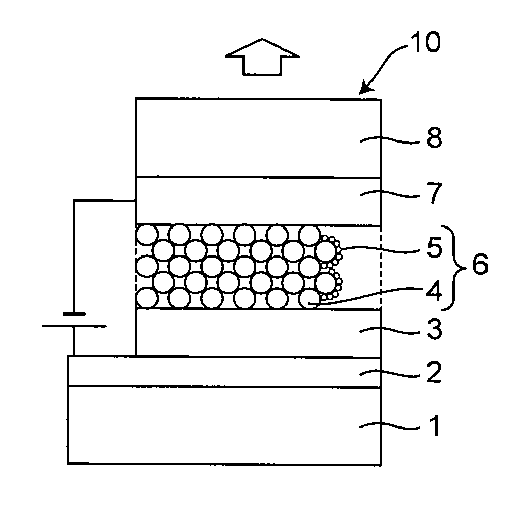
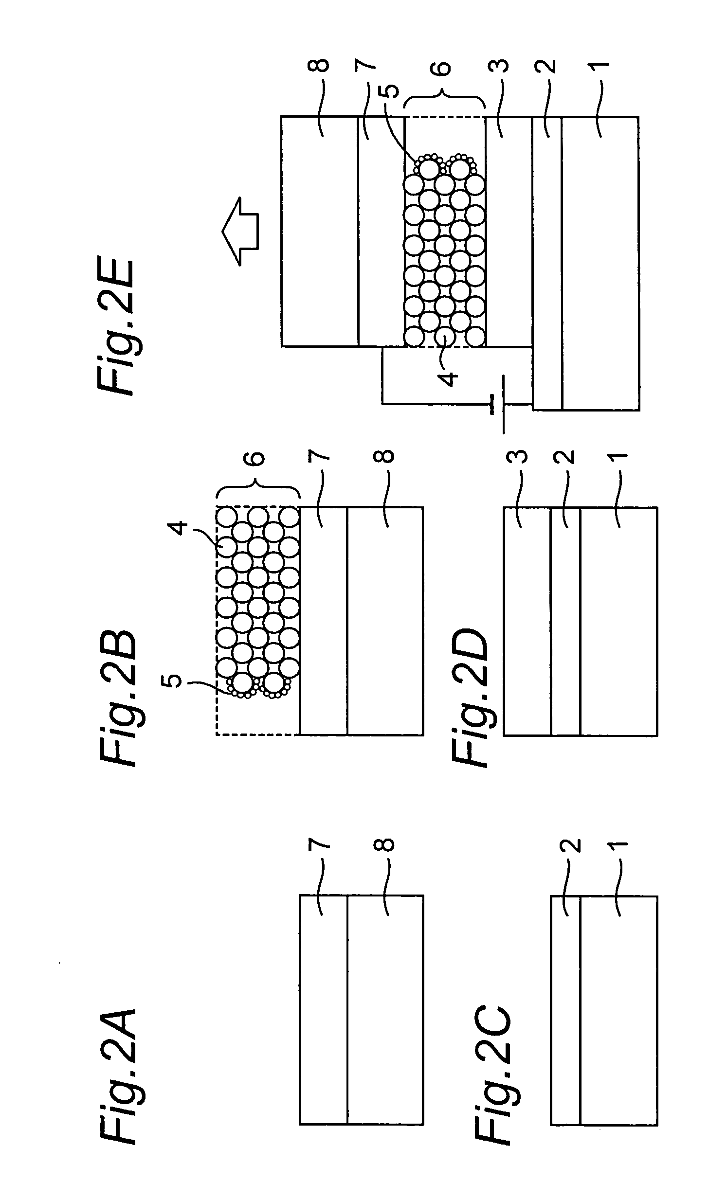
[0182] A light-emitting device according to an embodiment 1 of the present invention will be described with reference to FIG. 1. FIG. 1 is a cross-sectional view of a light-emitting device 10 taken along a plane perpendicular to a light-emitting surface thereof. The light-emitting device 10 uses an organic light-emitting material 5 as a light-emitting material. The light-emitting device 10 includes a transparent substrate 8, a substrate 1 provided so as to be opposed to the transparent substrate 8, and a light-emitting layer 6 which is provided between the transparent substrate 8 and the substrate 1 and contains a porous body composed of metal oxide semiconductor fine particles 4 by the surface of which the organic light-emitting material 5 is supported. More specifically, the light-emitting device 10 further includes a transparent electron injection electrode 7 provided on the transparent substrate 8, a hole injection electrode 2 provided on the substrate 1, and a hole transport la...

embodiment 2

[0220] A light-emitting device according to an embodiment 2 of the present invention will be described with reference to FIG. 3. FIG. 3 is a perspective view which shows the structure of electrodes of a light-emitting device 20. The light-emitting device 20 further includes a thin film transistor 21 connected to the hole injection electrode 2. To the thin film transistor 21, an x electrode 22 and a y electrode 23 are also connected. The light-emitting device 20 can have a high aperture ratio irrespective of the placement of the thin film transistor 21 on the substrate 1 because light is take out of the light-emitting device from the transparent substrate 8 side. Further, the use of the thin film transistor 21 allows the light-emitting device 20 to have a memory function. As such a thin film transistor 21, a low-temperature polysilicon thin film transistor, or an amorphous silicon thin film transistor, or the like can be used. Alternatively, the thin film transistor 21 may be an orga...

embodiment 3

[0221] A display according to an embodiment 3 of the present invention will be described with reference to FIG. 4. FIG. 4 is a schematic plane view which shows an active matrix of a display 30 composed of a plurality of x electrodes 22 and a plurality of y electrodes 23 intersecting at right angles with the X electrodes 22. The display 30 is an active matrix display having a plurality of thin film transistors. The active matrix display 30 includes a light-emitting device array in which the plurality of light-emitting devices according to the embodiment 2 shown in FIG. 3 are two-dimensionally arrayed, the plurality of x electrodes 22 extending in parallel with each other in a first direction parallel to the surface of the light-emitting device array, and the plurality of y electrodes 23 extending in parallel with each other in a second direction parallel to the surface of the light-emitting device array and orthogonal to the first direction. Each of the thin film transistors 21 of th...


PUM

PropertyMeasurementUnit
particle diameteraaaaaaaaaa
luminanceaaaaaaaaaa
thicknessaaaaaaaaaa

Abstract

Disclosed herein is a light-emitting device comprising a transparent or semi-transparent first substrate, a second substrate provided opposite to the first substrate, a transparent or semi-transparent first electrode provided on the first substrate, a second electrode provided on the second substrate so as to be opposite to the first electrode, and a light-emitting layer which contains a metal oxide semiconductor porous body, by the surface of which an organic light-emitting material is supported, and is provided between the first electrode and the second electrode.

Description

FIELD OF THE INVENTION [0001] The present invention relates to a light-emitting device which can be used as a light source for various applications such as light-emitting displays, communications, and lighting, and a display using the light-emitting device. BACKGROUND ART [0002] In recent years, attention is being given to flat displays, especially to electroluminescence (hereinafter, simply referred to as “EL”) devices. The EL devices are self-emission type devices, and thus have advantages such as high visibility, wide viewing angles, and high responsivity. [0003] The EL devices now practically used include inorganic EL devices using inorganic light-emitting materials and organic EL devices using organic light-emitting materials. Inorganic EL devices using inorganic materials such as zinc sulfide require a relatively high alternating voltage to operate, and therefore driving circuits thereof are likely to be complicated. In addition, such inorganic EL devices have a problem that b...

Claims


Application Information

Patent Timeline
Patent Type & Authority Applications(United States)
IPC IPC(8): H01L33/00H01L27/32H01L51/50H05B33/02H05B33/04H05B33/10H05B33/14H05B33/26
CPCH01L51/5012H01L27/3244H10K59/12H10K50/11
Inventor ONO, MASAYUKIHORI, KENYAAOYAMA, TOSHIYUKIODAGIRI, MASARUNAGO, KUMIOHASEGAWA, KENJI
Owner PANASONIC CORP
Why Eureka
Try Eureka