Light-emitting organic compound and EL display device utilizing the same

a technology of organic compound and display device, which is applied in the direction of organic semiconductor devices, discharge tube luminescnet screens, other domestic articles, etc., can solve the problems of increasing current flow, increasing the amount of heat generation, and reducing the resistance value of the light-emitting layer, so as to prevent the deterioration caused by unnecessary heat generation and high reliability. , the effect of high reliability

Inactive Publication Date: 2007-01-11
SEMICON ENERGY LAB CO LTD
View PDF37 Cites 76 Cited by
  • Summary
  • Abstract
  • Description
  • Claims
  • Application Information

AI Technical Summary

Benefits of technology

[0008] The present invention is intended to provide an EL display device with high reliability. The present invention is also intended to provide an electronic apparatus with a highly reliable display portion by utilizing such an EL display device as its display portion.
[0013] On the other hand, when a light-emitting organic compound made of a high-molecular compound (hereinafter, referred to as the high-molecular type EL compound) is used, values of molecular weight are likely to vary over a certain range since degree of polymerization cannot be completely controlled. Thus, a melting temperature of the resultant material cannot be decided unambiguously at a certain value, and therefore, it becomes difficult to perform purification. In this case, it is appropriate to perform a dialysis method or a high-performance liquid chromatography method. In particular, it is appropriate to perform an electrodialysis method for efficiently eliminating ionic impurities in the dialysis method.
[0029] In accordance with the present invention, a solvent containing a high-molecular type EL compound is applied by means of a spinner, and a heat treatment is then performed at a temperature that is sufficiently low for preventing crystallization of the high-molecular type EL compound (specifically, at a glass-transition temperature or lower) so as to volatilize the solvent. As a result, a thin film made of the high-molecular type EL compound can be formed on the substrate.
[0032] With the above-mentioned structure, a current that is caused by reasons other than the carrier recombination can be prevented from flowing through a thin film made of the light-emitting organic compound that is contained in an EL device, and deterioration caused by unnecessary heat generation can be prevented. Accordingly, it is possible to obtain an EL display device with high reliability. Moreover, an electronic apparatus with a highly reliable display portion can be obtained by utilizing such an EL display device as its display portion.

Problems solved by technology

In a light-emitting element such as a light-emitting diode in which a semiconductor junction is formed, Na (sodium) that may exhibit an adverse effect as a movable ion causes a resistance value of the light-emitting layer to decrease, and therefore, can cause a current flow other than that caused by the carrier recombination.
When such an unnecessary current flows, an amount of heat generation is increased and the light-emitting layer is more likely to deteriorate.
The same disadvantage may occur in the EL device.
However, any sufficient countermeasure against the disadvantage caused by the movable ion has not been provided for the EL material.

Method used


Image

  • Light-emitting organic compound and EL display device utilizing the same
  • Light-emitting organic compound and EL display device utilizing the same
  • Light-emitting organic compound and EL display device utilizing the same

Examples


embodiment 1

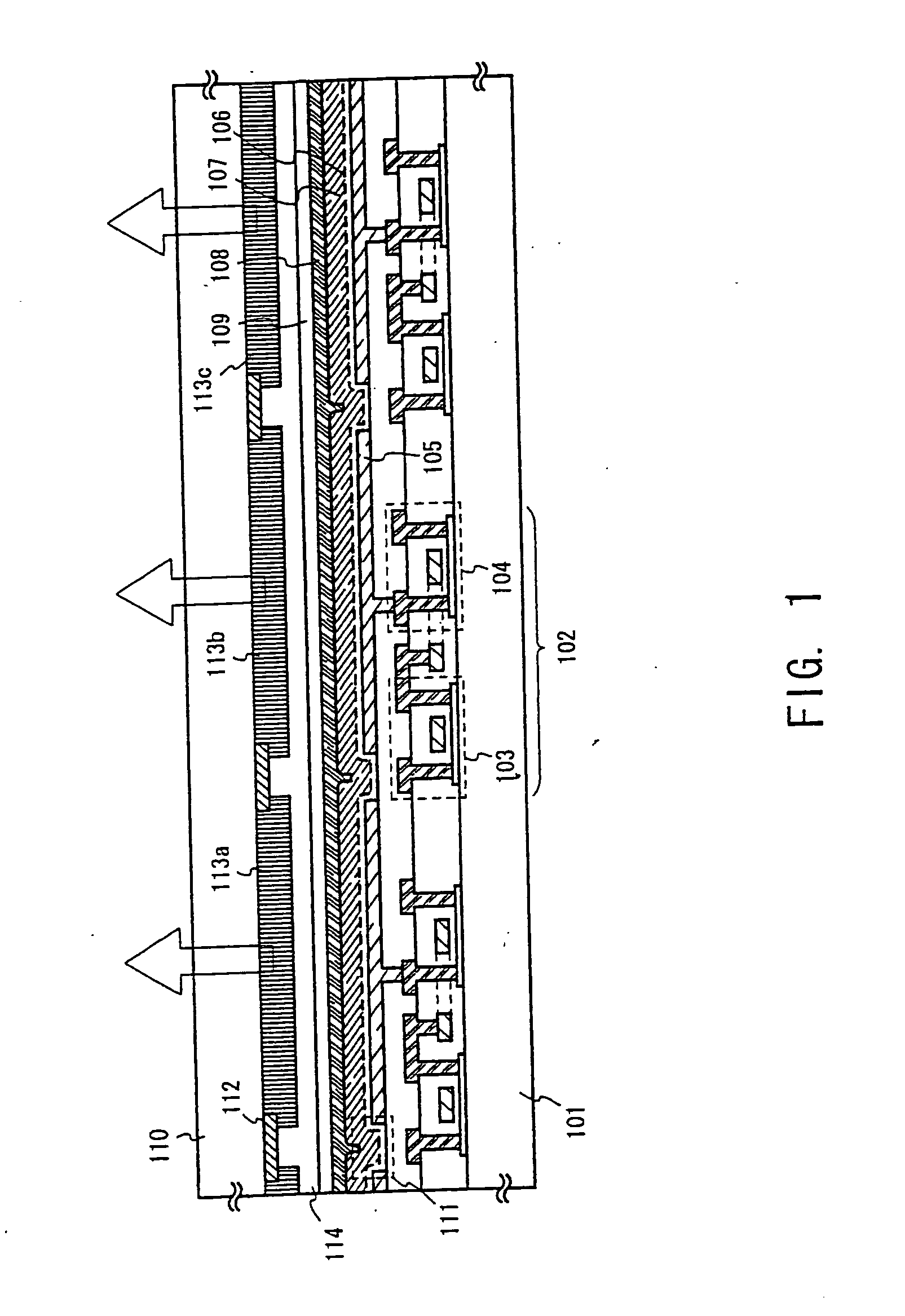
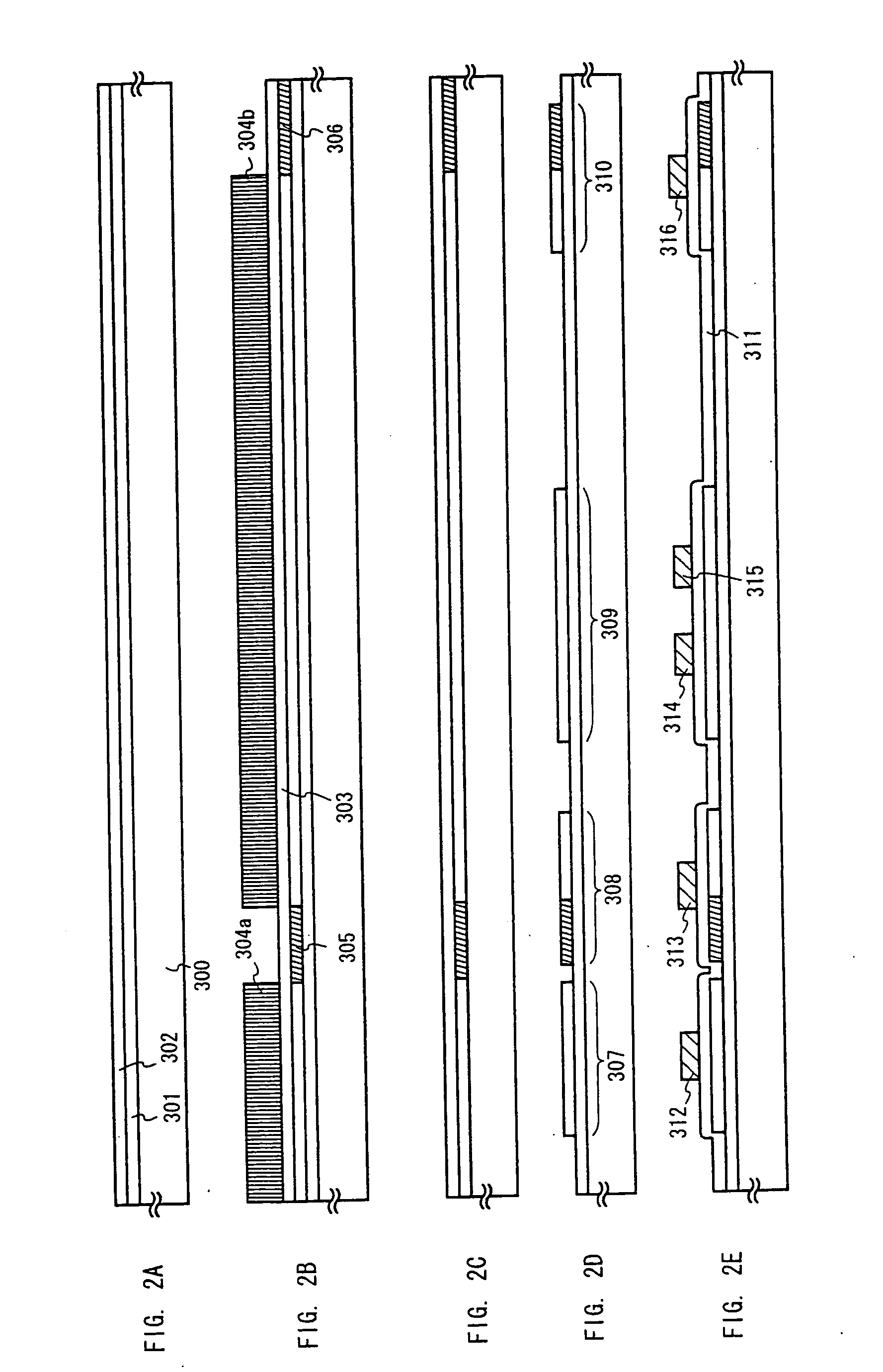
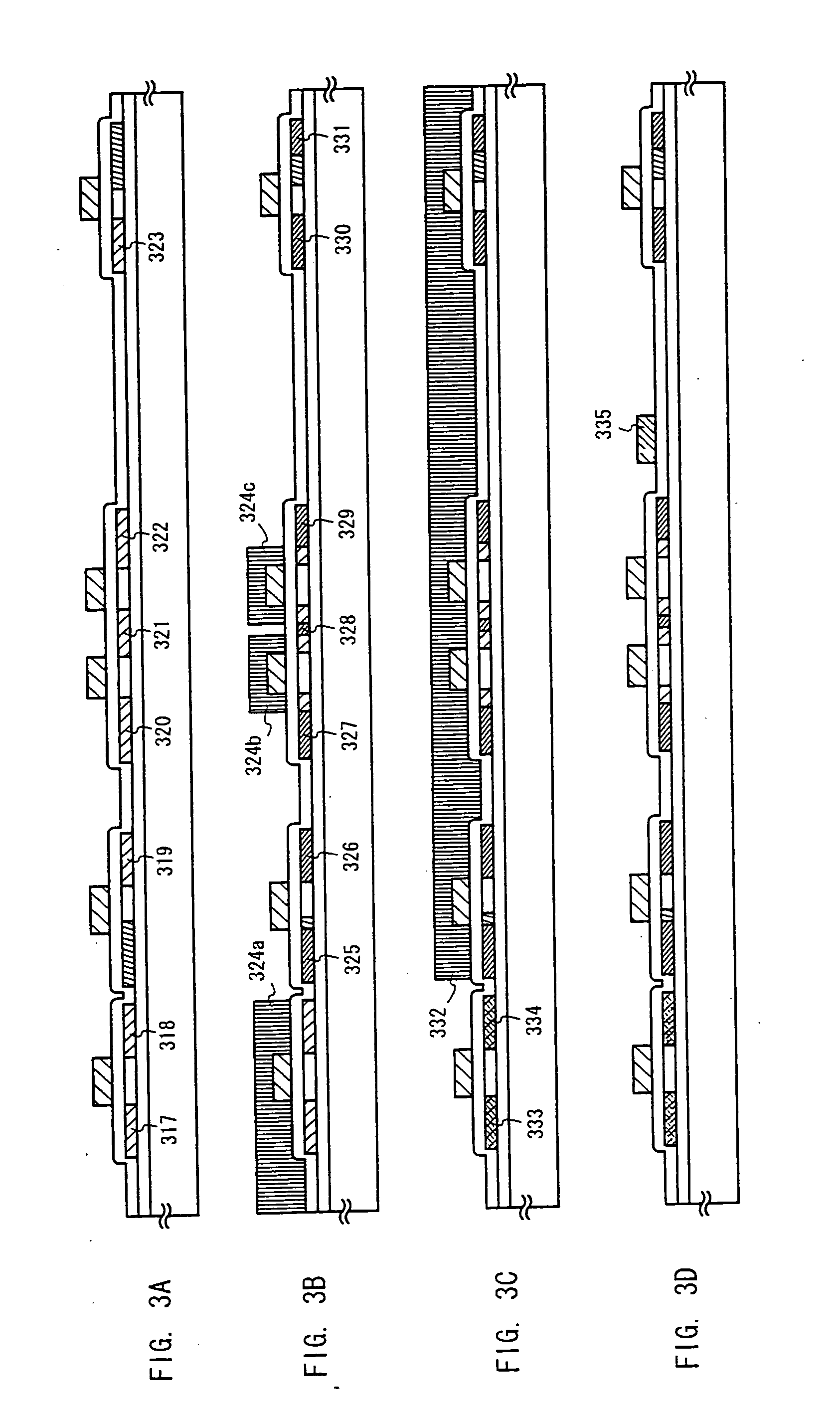
[0075] A first embodiment of the invention is described here. A description will be made here on a method for fabricating TFTs of a pixel portion and driving circuit portions provided around the same simultaneously. For simplicity of the description, only a CMOS circuit is shown which is a basic circuit for such driving circuits.

[0076] First, as shown in FIG. 2A, an base film 301 having a thickness of 300 nm is formed on a glass substrate 300. In the present embodiment, the a silicon oxinitride film is laminated as the base film 302. At this time, the density of nitrogen in the region in contact with the glass substrate 300 is preferably in the range from 10 to 25 wt %.

[0077] Next, an amorphous silicon film (not shown) having a thickness of 50 nm is formed on the base film 301 using a known film forming method. The film is not limited to an amorphous silicon film, and it may be any semiconductor film (and any microcrystalline semiconductor film) including an amorphous structure. T...

embodiment 2

[0145] In the present embodiment, the case where the present invention is applied to a simple-matrix type EL display device will be described with reference to FIG. 7. In FIG. 7, reference numeral 701 denotes a plastic substrate, 702 denotes a cathode made of a layered structure including an aluminum film and a lithium fluoride film (more specifically, the lithium fluoride film is provided so as to be in contact with the EL layer). In the present embodiment, the cathode 702 is formed by the vapor deposition method. Although not illustrated in FIG. 7, a plurality of the cathodes are arranged in stripes along in a direction perpendicular to the drawing sheet.

[0146] On the cathode 702, an EL layer 703 (only including a light-emitting layer) made of a high-molecular type EL compound is formed by the printing method. In the present embodiment, PVK (polyvinylcarbazole), Bu-PBD (2-(4′-tert-butyl phenyl)-5-(4″-biphenyl)-1,3,4-oxydiazole), coumarin6, DCM1 (4-dicyanomethylene-2-methyl-6-p-di...

embodiment 3

[0154] The EL display device fabricated in accordance with the present invention is of the self-emission type, and thus exhibits more excellent recognizability of the displayed image in a light place as compared to the liquid crystal display device. Furthermore, the EL display device has a wider viewing angle. Accordingly, the EL display device can be applied to a display portion in various electronic devices. For example, in order to view a TV program or the like on a large-sized screen, the EL display device in accordance with the present invention can be used as a display portion of an EL display (i.e., a display in which an EL display device is installed into a frame) having a diagonal size of 30 inches or larger (typically 40 inches or larger.)

[0155] The EL display includes all kinds of displays to be used for displaying information, such as a display for a personal computer, a display for receiving a TV broadcasting program, a display for advertisement display. Moreover, the ...


PUM


Abstract

By repeating a purification process of a light-emitting organic compound several times, a thin film made of the light-emitting organic compound to be used in an EL display device contains ionic impurities at the concentration of 0.1 ppm or lower and has a volume resistivity in the range of 3×10¹⁰ Ωcm or larger. By using such a thin film as a light-emitting layer in the EL device, a current caused by reasons other than the carrier recombination can be prevented from flowing through the thin film, and deterioration caused by unnecessary heat generation can be suppressed. Accordingly, it is possible to obtain an EL display device with high reliability.

Description

BACKGROUND OF THE INVENTION [0001] 1. Field of the Invention [0002] The present invention relates to a light-emitting organic compound (including a complex that contains a metal in its molecular formula) capable of providing Electro Luminescence (EL), and an EL display device utilizing the same. Typically, the present invention relates to a high-molecular type EL display device which utilizes a light-emitting organic compound made of a high-molecular compound. [0003] The present invention also relates to an electronic apparatus including the above-mentioned EL display device as its display portion. It should be noted that the above-mentioned EL display device will be also referred to as the OLED (Organic Light-emitting Diode). [0004] 2. Description of the Related Art [0005] Development of a display device including an EL layer as a self-light emitting element that utilizes EL phenomenon (i.e., the EL display device) has been proceeded in these years. Since the EL display device is o...

Claims


Application Information

Patent Timeline
Patent Type & Authority Applications(United States)
IPC IPC(8): H01L51/52H05B33/02H01L27/32H01L51/00H01L51/30H01L51/50
CPCH01L27/32H01L27/322H01L27/3244H01L51/0025H01L51/0035H01L51/0038Y10S428/917H01L51/0081H01L51/5012H01L51/5237H01L51/5284H01L2251/5315H01L51/005H10K59/38H10K59/00H10K71/311H10K59/12H10K85/111H10K85/114H10K85/60H10K85/324H10K50/8423H10K50/846H10K50/8426H10K50/865H10K50/11H10K2102/3026H10K50/844H10K50/84
Inventor YAMAZAKI, SHUNPEIKONUMA, TOSHIMITSUMIZUKAMI, MAYUMI
Owner SEMICON ENERGY LAB CO LTD
Why Eureka
Try Eureka