

Method for manufacturing semiconductor device
a manufacturing method and semiconductor technology, applied in the field of semiconductor device manufacturing, can solve the problems of easy generation of cracks and peeling in resin bm, long exposure time, light transmissivity, etc., and achieve the effect of improving brightness or color contrast, and suppressing cracks and peeling
- Summary
- Abstract
- Description
- Claims
- Application Information
AI Technical Summary
Benefits of technology
Problems solved by technology
Method used
Image

Examples
embodiment 1
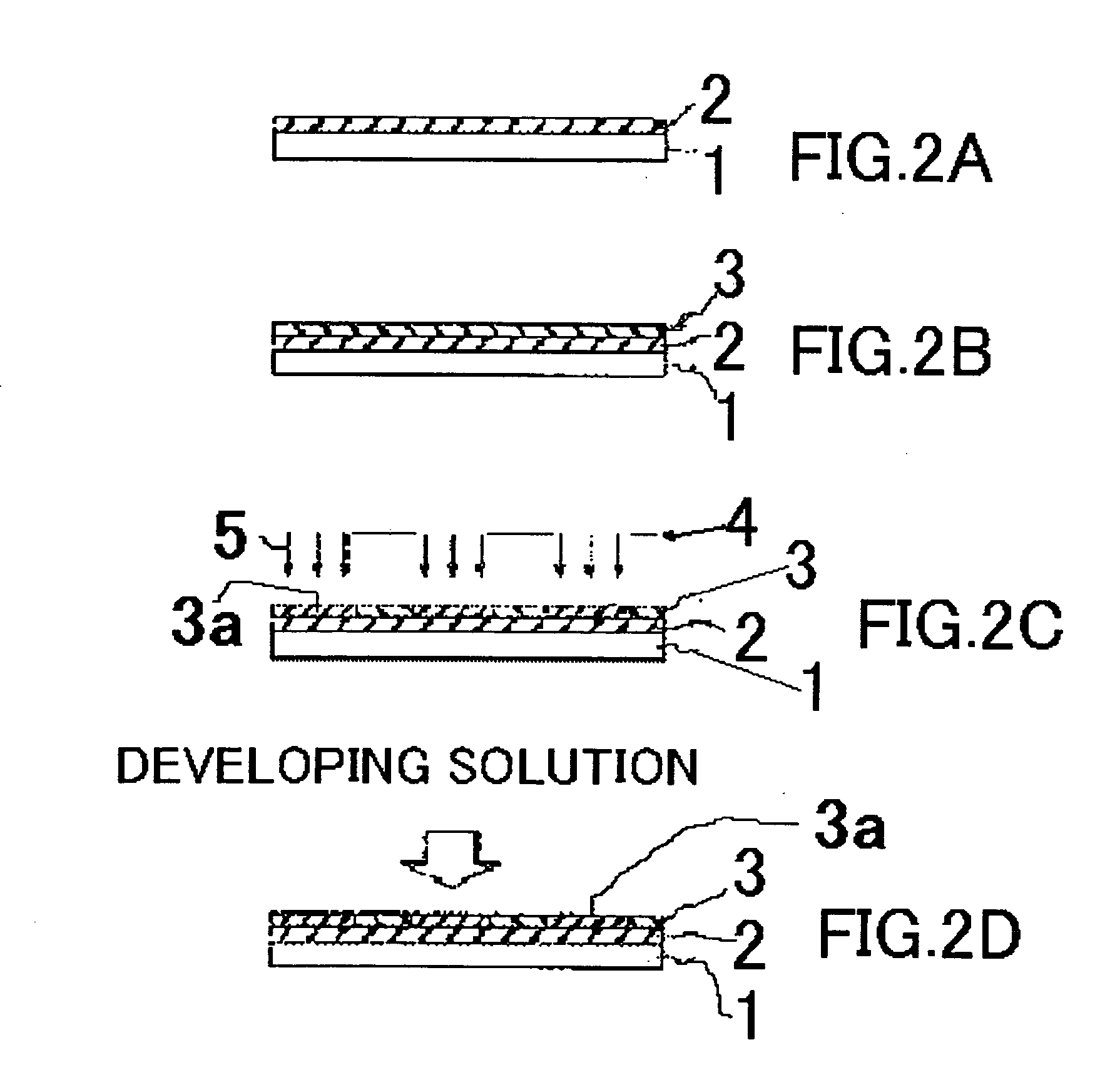
[0055]FIGS. 6A to 6E show cross-sectional views for showing a method for manufacturing a semiconductor device in accordance with Embodiment 1 of the present invention.
[0056] First, as shown in FIG. 6A, a base insulating film 101 is formed over a substrate 100. Here, as the substrate 100, a glass substrate, a quartz substrate, a ceramic substrate, or the like can be used. Further, as the substrate, an insulting film may be formed on a surface of a silicon substrate, a metal substrate, or a stainless substrate. Furthermore, a plastic substrate that can thermally withstand a processing temperature in all of the following steps.
[0057] The base insulating film 101 is provided to prevent an element (for example, an alkali metal) contained in the substrate 100 from being dispersed into a semiconductor film formed in the upper layer of the substrate 100. As the base insulating film 101, an insulating film such as a silicon oxide film, a silicon nitride film, or a silicon oxynitride film (...
embodiment 2
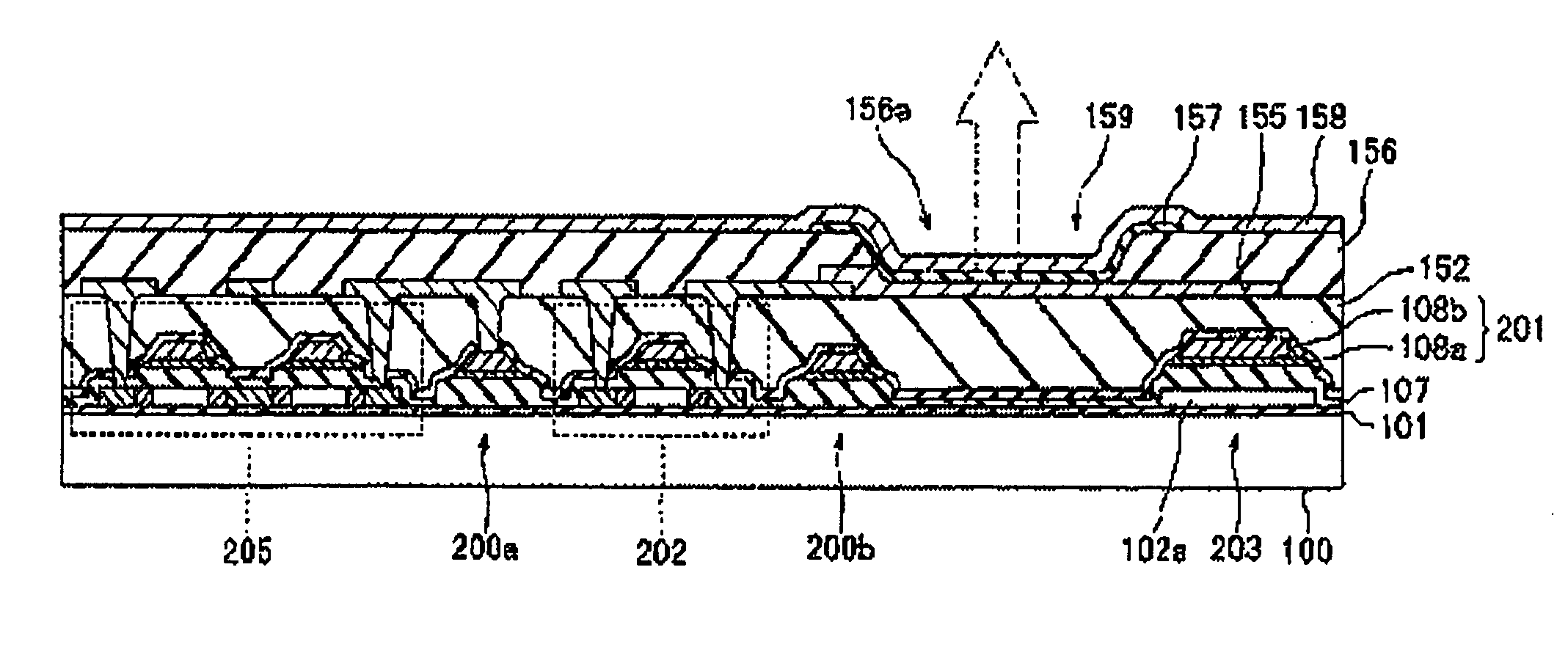
[0089]FIG. 7 shows a cross-sectional view for explaining a method for manufacturing a semiconductor device in according with Embodiment 2 of the present invention. The same portion as FIGS. 6A to 6E are denoted by the same reference numeral, and only different portions will be explained. This semiconductor device is an EL light emitting device manufactured by using a resin BM as a partition.
[0090] A first TFT 205 and a second TFT 202 are formed over a base insulating film 101. Each of the first TFT 205 and the second TFT 202 is manufactured by the same steps as that of the TFT 204 in Embodiment 1.
[0091] A capacitor element 203 including a lower electrode 102a, a gate insulating film 107, and an upper electrode 201 is formed over the base insulating film 101. This capacitor element 203 is manufactured in the steps of forming the TFT 204 in Embodiment 1. In other words, the lower electrode 102a of the capacitor element is manufactured in the step of forming the crystalline semicondu...
embodiment 3
[0097] In this embodiment, a method for manufacturing a light emitting display device provided with an electroluminescent element, which is formed by Embodiment 1 or 2, will be explained. An electroluminescent element is, for example, an EL (Electro Luminescence) element, which includes an organic light emitting layer including an organic compound (an organic light emitting material) that emits light by adding the electric field, an anode, and a cathode. As for a light emitting display device using an electroluminescent element, a TFT is a required element so as to realize an active matrix driving method. In other words, in the light emitting display device using the electroluminescent element, a TFT serving as a switching element and a TFT supplying a-current to the electroluminescent element are at least provided in each pixel.
[0098] In this light emitting display device, in order to make a clear difference of light and dark in an image and to display black color more vividly, a ...
PUM
| Property | Measurement | Unit |
|---|---|---|
| thickness | aaaaa | aaaaa |
| temperature | aaaaa | aaaaa |
| temperature | aaaaa | aaaaa |
Abstract
Description
Claims
Application Information