White organic light emitting diode

a light-emitting diode and organic technology, applied in the direction of discharge tube/lamp details, luminescnet screens, discharge tubes, etc., can solve the problems of deterioration of the stability short life of the white oled, and the acquisition of thin film emitted by the white light, so as to improve the emission efficiency and prolong the life

Inactive Publication Date: 2007-01-18
SAMSUNG MOBILE DISPLAY CO LTD
View PDF4 Cites 87 Cited by
  • Summary
  • Abstract
  • Description
  • Claims
  • Application Information

AI Technical Summary

Benefits of technology

[0009] In one embodiment, the invention provides a white organic light emitting diode (OLED) with improved emission efficiency and a longer lifespan wherein at least one of the materials that has hole transporting properties and at least one material that has electron transporting properties are used in an emission layer.

Problems solved by technology

Using this method, it is not easy to form the multiple layers, the thickness of the thin film that emits white light must be obtained through trial and error without regulations, the color of light significantly changes in accordance with voltage, and the stability of the white OLED deteriorates, thereby producing a white OLED with a very short life.
However, according to the second method, the thin film that emits the white light is also obtained through trial and error.

Method used


Image

  • White organic light emitting diode
  • White organic light emitting diode
  • White organic light emitting diode

Examples


example 1

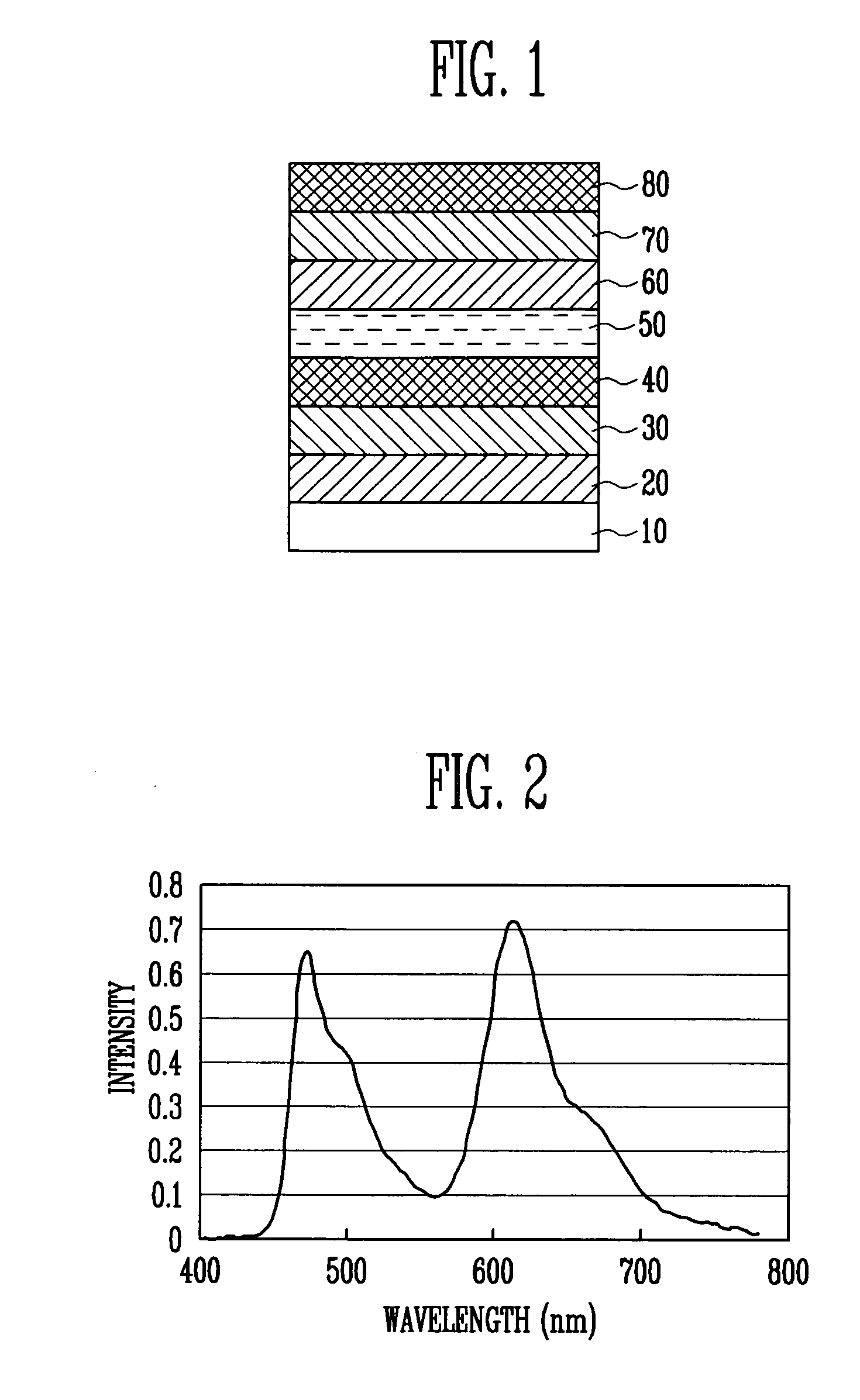
[0051] An ITO glass substrate of 15 Ω / cm2 (1,200 Å) obtained from Corning Inc. is cut to a size of 50 mm×50 mm×0.7 mm and is ultrasonically cleaned under a solution of isopropyl alcohol and pure water for 5 minutes and then is UV and ozone cleaned for 30 minutes. After the cleaning process, the ITO glass substrate is plasma processed under a vacuum of no more than 0.1 mtorr for 9 minutes.

[0052] IDE406 from Idemitsu Co., LTD is vacuum thermal deposited on the substrate to form the hole injecting layer with a thickness of 700 Å. Then, α-NPD is vacuum thermal deposited on the hole injecting layer with a thickness of 150 Å to form the hole transporting layer.

[0053] A 1:1 mixture of CBP(4,4′-biscarbazolylbiphenyl) and BCP(2,9-dimethyl-4,7-diphenyl-9,10-phenanthroline) as the host is doped with 15 wt % FIrpic as the blue dopant and 3 wt % Irqp2acac as the yellow dopant to form a 400 Å thick emission layer on the hole transporting layer by vacuum thermal deposition.

[0054] Then Alq3, whi...

example 2

[0055] An ITO glass substrate of 15 Ω / cm2 (1,200 Å) obtained from Corning Inc. is cut to a size of 50 mm×50 mm×0.7 mm and is ultrasonically cleaned under a solution of isopropyl alcohol and pure water for 5 minutes and then is UV and ozone cleaned for 30 minutes. After the cleaning process, the ITO glass substrate is plasma processed under a vacuum of no more than 0.1 mtorr for 9 minutes.

[0056] IDE406 from Idemitsu Co., LTD is vacuum thermal deposited on the substrate to form the hole injecting layer with a thickness of 700 Å. Then, α-NPD is vacuum thermal deposited on the hole injecting layer with a thickness of 150 Å to form the hole transporting layer.

[0057] A 1:1 mixture of CBP and BCP as the host is doped with 2 wt % Ir(piq)2acac as the red dopant, 3 wt % Irppy3 as the green dopant, and 15 wt % FIrpic as the blue dopant to form a 400 Å thick emission layer on the hole transporting layer by vacuum thermal deposition.

[0058] Then Alq3, which is the electron transporting materia...

experimental example 1

[0067] The driving voltage, efficiency (current density), and half life of the white OLEDs manufactured in accordance with the Examples 1 and 2 and the Comparative Examples 1 and 2 were examined by the following methods and the results are described in Table 1.

[0068] Brightness was measured by a BM5A (Topcon).

[0069] Driving voltage was measured by a 238 HIGH CURRENT SOURCE MEASURE UNIT from Keithley.

[0070] Current density was measured by increasing DC from 10 to 100 mA / cm2 by 10 mA / cm2 increments, and was measured at no less than 9 points in the same OLED.

[0071] Half life was measured by investigating the time required to reduce the brightness of each of the OLEDs to 50% of the initial value when the same current density of DC 50 mA / cm2 is applied. Reproducibility of half life was confirmed by three or more OLEDs having the same structure.

[0072] Chromaticity coordinate was confirmed by PR650 spectrometer.

TABLE 1DrivingEfficiencyChromaticityvoltage (V)(cd / v)Half life (h)(CIEx ...


PUM

PropertyMeasurementUnit
thicknessaaaaaaaaaa
thicknessaaaaaaaaaa
thicknessaaaaaaaaaa

Abstract

A white organic light emitting diode (OLED) includes an emission layer between two electrodes. The emission layer comprises two or more kinds of compounds for the host and two or more kinds of compounds for the dopant that facilitate production of a white color. Among the two or more kinds of compounds for the host, at least one is a hole transporting material and the other is an electron transporting material. The white OLED has improved stability which increases its efficiency and life.

Description

CROSS-REFERENCE TO RELATED APPLICATIONS [0001] This application claims priority to and the benefit of Korean Patent Application No. 2004-64460, filed on Jul. 15, 2005, in the Korean Intellectual Property Office, the entire content of which is incorporated herein by reference. BACKGROUND [0002] 1. Field of the Invention [0003] The present invention relates to a white organic light emitting diode (OLED) in which the structure of the emission layer is improved, thereby increasing the life of the white OLED. [0004] 2. Discussion of Related Art [0005] In general, an organic light emitting diode (OLED) includes a substrate, an anode, an organic layer including an emission layer, and a cathode. The OLED is a spontaneous emission display that generates light by a combination of electrons and holes in the emission layer, realizing a light and thin information display device that is driven at a low voltage, displays images with high picture quality, has high response speed, and has a wide vie...

Claims


Application Information

Patent Timeline
Patent Type & Authority Applications(United States)
IPC IPC(8): H01L51/54H05B33/14
CPCC09K11/06C09K2211/1007C09K2211/1014C09K2211/1029C09K2211/1044H05B33/14C09K2211/186H01L51/0072H01L51/0081H01L51/0085H01L51/5036C09K2211/181H10K85/324H10K85/6572H10K85/342H10K50/125
Inventor LEE, JUN YEOBCHUN, MIN SEUNG
Owner SAMSUNG MOBILE DISPLAY CO LTD
Why Eureka
Try Eureka