Manufacture method for semiconductor device having improved copper diffusion preventive function of plugs and wirings made of copper or copper alloy and semiconductor device of this kind
a manufacturing method and technology of a semiconductor device, applied in the direction of semiconductor devices, semiconductor/solid-state device details, electrical apparatus, etc., can solve the problems of copper film not adhesion enough to an insulating film, copper is likely to diffuse into an insulating film, and is easy to short circuit, etc., to improve the diffusion preventive function and good reproductivity
- Summary
- Abstract
- Description
- Claims
- Application Information
AI Technical Summary
Benefits of technology
Problems solved by technology
Method used
Image

Examples
first embodiment
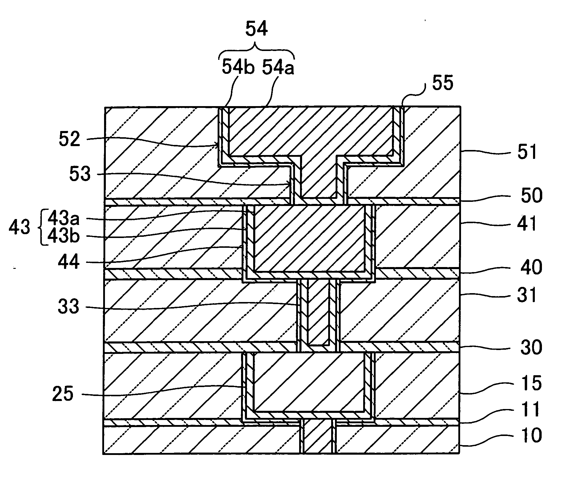
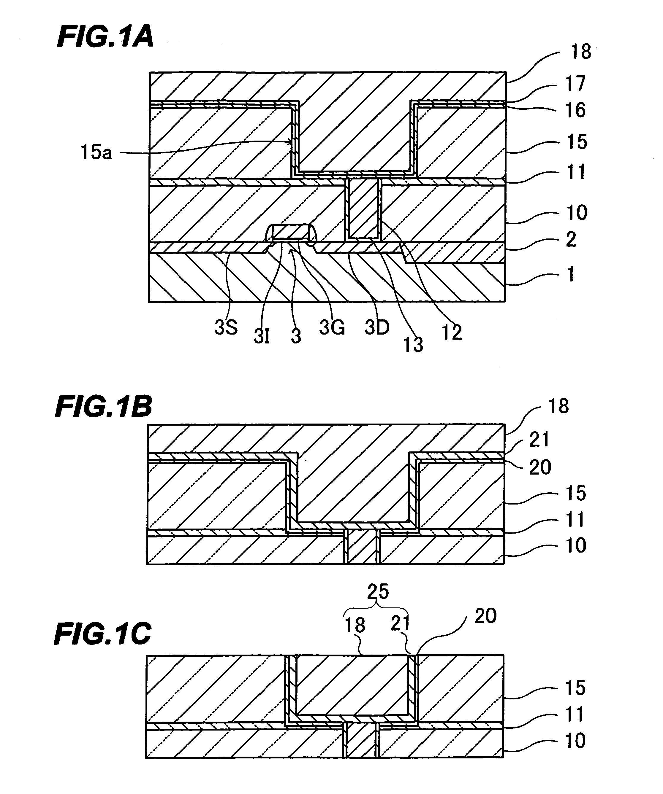
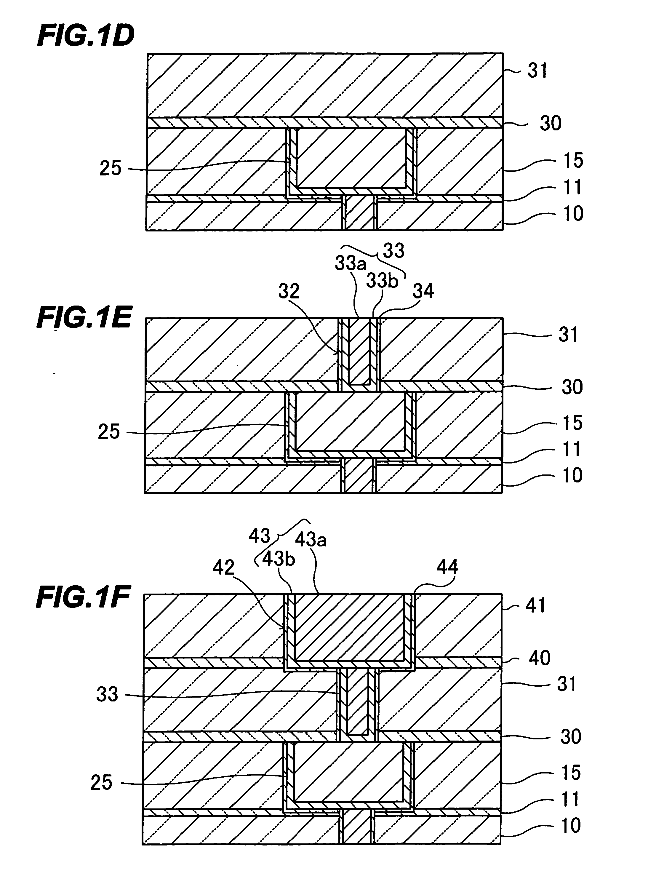
[0029] With reference to FIGS. 1A to 1G, description will be made on a semiconductor manufacture method according to the
[0030] As shown in FIG. 1A, an element isolation insulating film 2 of a shallow trench isolation (STI) structure is formed in a surface layer of a semiconductor substrate 1 of silicon to define active regions. A MOS transistor 3 is formed in an active region. The MOS transistor 3 is constituted of a source region 3S, a drain region 3D, a gate insulating film 31 and a gate electrode 3G.
[0031] An interlayer insulating film 10 of silicon oxide having a thickness of 300 nm and a protective film 11 of SiOC having a thickness of 50 nm are formed on the semiconductor substrate 1, covering the MOS transistor 3. A via hole is formed through the protective film 11 and interlayer insulating film 10, a partial surface of the drain region 3D being exposed on the bottom of the via hole. A conductive plug 13 of tungsten (W) is embedded in the via hole. A barrier metal layer 12 o...
second embodiment
[0056] Next, with reference to FIGS. 2A to 2C, description will be made on a semiconductor device manufacture method according to the
[0057] The structure of the protective film 11 and underlying layers shown in FIG. 2A is the same as that of the first embodiment shown in FIG. 1A. In the second embodiment, a single third film 60 is formed instead of the two films, the first film 16 and second film 17 of the first embodiment formed by the process shown in FIG. 1A. The structure of the interlayer insulating film 15 and metal film 18 is the same as that of the first embodiment.
[0058] The third film 60 is made of three-element copper alloy containing two types of alloy elements other than copper and can be formed by sputtering or chemical vapor deposition. The alloy elements are the same as those of copper alloy of the first film 16 and second film 17 of the first embodiment. A thickness of the third film 60 is almost equal to the total thickness of the first film 16 and second film 17 ...
third embodiment
[0069] Next, with reference to FIGS. 3A to 3D, description will be made on a semiconductor device manufacture method according to the
[0070] The structure of the protective film 11 and underlying layers shown in FIG. 3A is the same as that of the first embodiment shown in FIG. 1A. On the protective film 11, an interlayer insulating film 15 is formed and a wiring trench 15a is formed in the interlayer insulating film 15. The interlayer insulating film 15 is made of the same material as that of the interlayer insulating film 15 of the first embodiment shown in FIG. 1A. A barrier metal layer 70 is formed covering the inner surface of the wiring trench 15a and the upper surface of the interlayer insulating film 15, the barrier metal layer being made of refractory metal, alloy containing refractory metal or nitride of refractory metal. Refractory metal may be Ta, Ti, W or the like. The barrier metal layer 70 can be deposited, for example, by sputtering or chemical vapor deposition.
[0071]...
PUM
| Property | Measurement | Unit |
|---|---|---|
| resistivity | aaaaa | aaaaa |
| thickness | aaaaa | aaaaa |
| thickness | aaaaa | aaaaa |
Abstract
Description
Claims
Application Information
 - Generate Ideas
- Intellectual Property
- Life Sciences
- Materials
- Tech Scout
- Unparalleled Data Quality
- Higher Quality Content
- 60% Fewer Hallucinations
Browse by: Latest US Patents, China's latest patents, Technical Efficacy Thesaurus, Application Domain, Technology Topic, Popular Technical Reports.
© 2025 PatSnap. All rights reserved.Legal|Privacy policy|Modern Slavery Act Transparency Statement|Sitemap|About US| Contact US: help@patsnap.com