Small object moving on printed circuit board

a printed circuit board and small object technology, applied in the field of manipulating small objects, can solve the problems of high operating voltage, power consumption and high operating voltage, complex, etc., and achieve the effects of improving the efficiency of the electrokinetic mechanism

Inactive Publication Date: 2007-02-01
RGT UNIV OF CALIFORNIA
View PDF8 Cites 374 Cited by
  • Summary
  • Abstract
  • Description
  • Claims
  • Application Information

AI Technical Summary

Benefits of technology

[0019] In another embodiment, a top plate is placed over the printed circuit board with spacers placed there between to form a space between the top plate and the PCB. The space forms the passage of the device having a driving surface. Depending on the configuration, the driving surface can be the surface of the electrodes, or a dielectric layer or low-friction layer if provided onto the surface of the electrodes. The electrode pads are configured to modify the surface wettability of the driving surface in response to an electrical potential being applied to one or more of the electrode pads. Selective application of an electrical potential to the desired electrode pads selectively modifies the surface wettability of the activated pads in order to manipulate droplets contained within the space. For example, droplets may be created from a reservoir, moved, divided, and / or mixed. The microfluidic device is completely reconfigurable and customizable to perform any desired series of functions on one or more droplets because each electrode pad can be independently controlled. Moreover, the independent control allows the straightforward, simultaneous manipulation of multiple droplets.

Problems solved by technology

These types of pumps utilize moving parts which may present problems related to manufacturability, complexity, reliability, power consumption and high operating voltage.
Electrokinetic mechanisms (i.e., electrophoresis and electroosmosis) are limited because to operating liquids that contain ionic particles.
Moreover, they require high voltage and high energy dissipation, and are relatively slow.
Dielectrophoresis requires asymmetric electric fields and lacks the design flexibility to serve as an actuation mechanism to generate continuous flows.
Likewise, magnetohydrodynamics and thermal bubble pumping require relatively high power to operate.
This leaves very little room to run electrical connection lines to each of the electrodes on the same surface of the substrate as the electrodes.
However, these types of chips do not allow for reconfigurability or user-customizable applications on single chip design.
Thus, even a somewhat small 2-D grid leaves little room on the grid surface for electrical connections.
However, this type of system presents functional limitations, such as the ability to simultaneously drive multiple droplets, which may require the development of a time-multiplexed driving scheme.
In addition, since all of the electrodes on both the top and bottom chips need to be connected to a control circuit, the electrical connection and device packaging are made more complex.
The droplet operation also requires multi-layer chips to be planarized, further increasing the chip cost.
As a result, the cost for such multilayer IC substrates is too high for typical microfluidic applications.

Method used


Image

  • Small object moving on printed circuit board
  • Small object moving on printed circuit board
  • Small object moving on printed circuit board

Examples


example

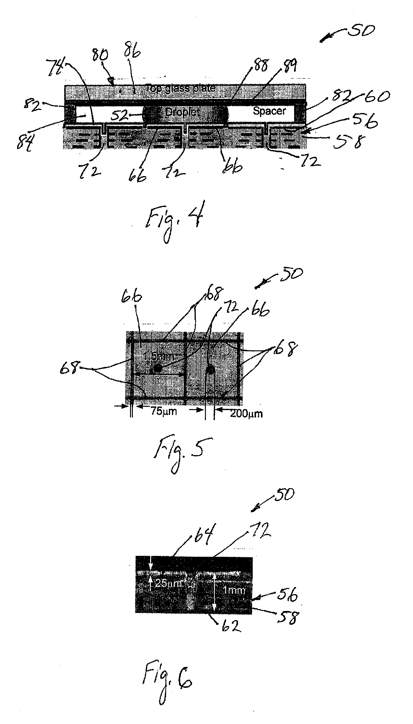
[0044] Referring to FIGS. 4-6, a specific example of a digital microfluidic system 50 according to the present invention will be described. The system 50 is physically configured as schematically shown in FIG. 4 and as described above. The PCB 56 has substrate 58 formed of FR4 and having an overall thickness of about 1 mm. The top conductive layer 64 is 25 μm thick copper. The array of electrode pads 66 formed by etching into an 8×8 rectangular array. Each electrode pad 66 has a square shape which is 1.5 mm wide. The gap 68 between the perimeter of each electrode 66 and the perimeter of each adjacent electrode is 75 μm. The vias 72 have a diameter of 200 μm.

[0045] The dielectric layer 70 is formed of a 5000 Angstrom (“Å”) thick layer of Parylene C applied by conformal, room temperature deposition. Over the dielectric layer, the hydrophobic layer 74 is a 2000 Å thick layer of FC75 AF1600 Teflon which is spin coated on top to make the surface more hydrophobic (resulting in a contact ...


PUM

PropertyMeasurementUnit
perimetersaaaaaaaaaa
thicknessaaaaaaaaaa

Abstract

A printed circuit board based digital or droplet microfluidic system and method for producing such microfluidic system are disclosed. The digital microfluidic device comprises a printed circuit board having a substrate and a plurality of electrode pads disposed on the top surface of the substrate in a rectangular array. A via extends from each electrode pad through the substrate to other locations on the substrate . A dielectric layer is disposed on the electrode pads. Droplets may be manipulated using electrowetting principles and others by applying a voltage to the desired electrodes. Each electrode pad can be controlled directly and independently from the other electrode pads to modify the surface wettability of the dielectric layer in the vicinity of the electrode pad by applying a voltage to the desired electrode pad(s). In this way, droplets may be formed, moved, mixed, and / or divided or other small objects manipulated while in air or immersed in a liquid on the dielectric surface.

Description

REFERENCE TO RELATED APPLICATIONS [0001] This Application claims the benefit, under 35 U.S.C. Section 119 and any other applicable laws, of U.S. Provisional Patent Application No. 60 / 702,367 filed on Jul. 26, 2005. U.S. Provisional Patent Application No. 60 / 702,367 is incorporated by reference as if set forth fully herein.STATEMENT REGARDING FEDERALLY SPONSORED RESEARCH AND DEVELOPMENT [0002] The U.S. Government may have a paid-up license in this invention and the right in limited circumstances to require the patent owner to license others on reasonable terms as provided for by the terms of Grant No. NCC2-1364 by the National Aeronautics and Space Administration.FIELD OF THE INVENTION [0003] The field of the invention generally relates to systems for manipulating small objects such as fluid droplets, and more particularly, to a system which utilizes a printed circuit board having a plurality of electrodes for exerting motive effects on small objects within the system. [0004] Backgro...

Claims


Application Information

Patent Timeline
Patent Type & Authority Applications(United States)
IPC IPC(8): B03C5/02
CPCB01F13/0076B01L3/502792B01L2300/0819F04B19/006B01L2400/0421B01L2400/0424B01L2400/0427B01L2300/089B01F33/3031
Inventor KIM, CHANG-JINGONG, JIAN
Owner RGT UNIV OF CALIFORNIA
Why Eureka
Try Eureka