SRAM cell with independent static noise margin, trip voltage, and read current optimization

a static noise margin and sram cell technology, applied in static storage, information storage, digital storage, etc., can solve the problems of increasing the difficulty of designing an sram cell, snm degradation, and no longer being able to achieve a balan

Active Publication Date: 2007-02-01
TEXAS INSTR INC
View PDF10 Cites 30 Cited by
  • Summary
  • Abstract
  • Description
  • Claims
  • Application Information

AI Technical Summary

Benefits of technology

[0009] The following presents a simplified summary in order to provide a basic understanding of one or more aspects of the invention. This summary is not an extensive overview of the invention, and is neither intended to identify key or critical elements of the invention, nor to delineate the scope thereof. Rather, the primary purpose of the summary is to present some concepts of the invention in a simplified form as a prelude to the more detailed description that is presented later. The invention relates to an SRAM memory cell structure (e.g., a 7 T single ended and a 10 T differential SRAM memory cell) utilizing a read driver transistor fo

Problems solved by technology

As transistor scaling trends continue, however, it becomes increasingly difficult to design an SRAM cell that has both adequate static noise margin (SNM) and adequate trip voltage (Vtrip), because of their interdependency in cell design.
Also, if the load is too weak relative to the drive transistor, SNM is degraded.
With technology scaling to the 45 nm node and beyond,

Method used


Image

  • SRAM cell with independent static noise margin, trip voltage, and read current optimization
  • SRAM cell with independent static noise margin, trip voltage, and read current optimization
  • SRAM cell with independent static noise margin, trip voltage, and read current optimization

Examples


Embodiment Construction

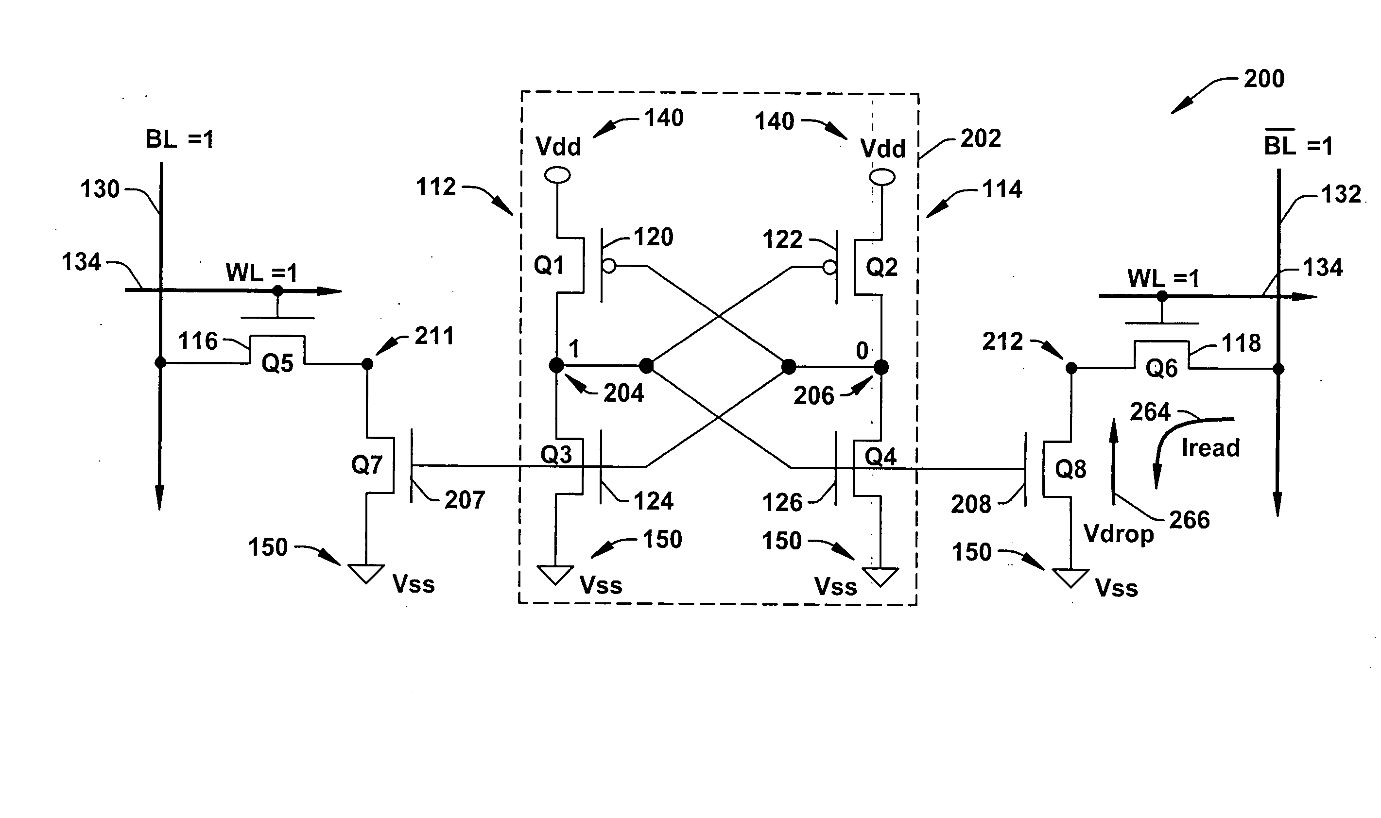
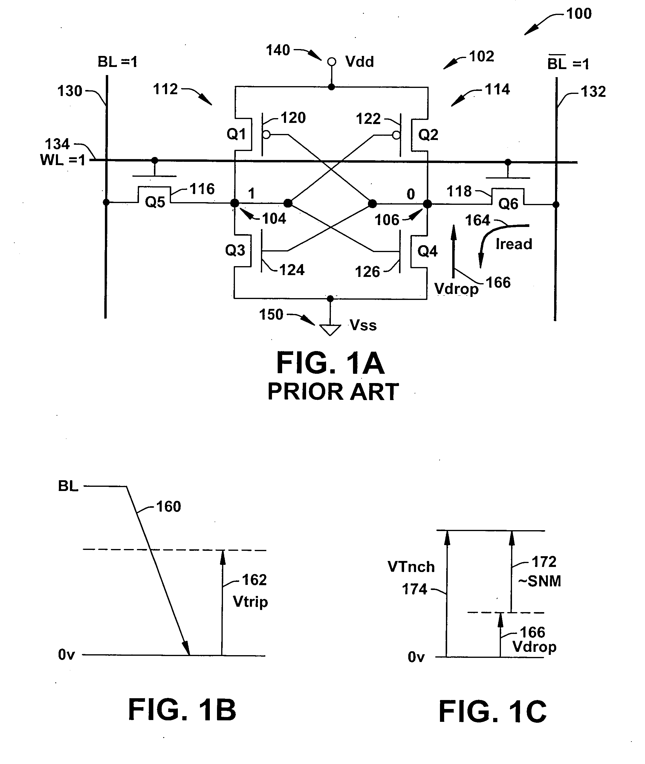
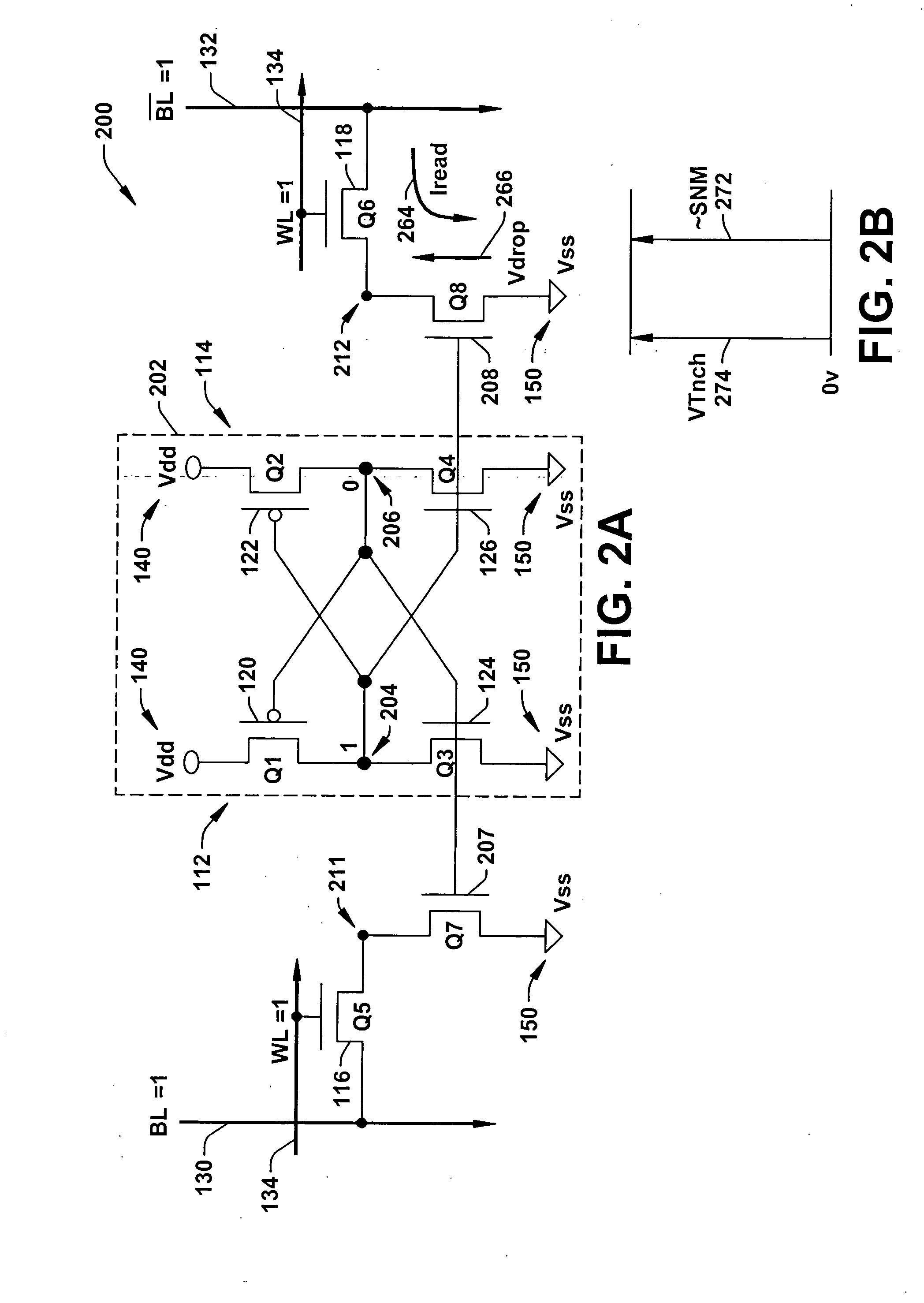
[0040] The present invention will now be described with reference to the attached drawings, wherein like reference numerals are used to refer to like elements throughout. The invention provides an SRAM memory cell structure (e.g., a 7 T single ended and a 10 T differential SRAM memory cell) utilizing a read driver transistor for removing or isolating the read current from the latch nodes (data nodes) of the data cell during read operations, and a column write transistor for selection of cell columns or a single cell during write operations. Because the read current is isolated from the data storage cell of the present invention, the static noise margin (SNM), trip voltage (Vtrip), and read current (Iread) may be independently optimized, thereby avoiding some of the static noise margin and trip voltage compromises and problems of conventional SRAM cells (e.g., a conventional 6 T differential cell).

[0041] As indicated previously, feature scaling trends continue down to around 45 nm a...


PUM


Abstract

An SRAM memory cell structure utilizing a read driver transistor for isolating the read current from the latch nodes of the cell during read operations and a column select write transistor for selection of a single cell during write operations, and a method of operating the same is discussed. The SRAM memory cell structure (single-ended or differential cell) allows independent optimization of the static noise margin, trip voltage, and read current, thereby avoiding some of the static noise margin and trip voltage problems of conventional SRAM cells (e.g., a conventional 6T differential cell). In one implementation, the SRAM memory cell comprises a 7T single-ended cell including first and second cross-coupled inverters, having a first and second latch nodes, respectively. The cell further comprises a first write pass transistor connected between the first latch node of the first inverter and a first pass node, and a first wordline pass transistor connected between the first pass node and a first bitline. The cell also includes a first read driver connected between the first pass node and a source potential, and a control terminal of the first read driver connected to the second latch node of the second inverter. Beneficially, the read current conducts through the first read driver to avoid upsetting the data state at the latch node. Further, a differential 10T SRAM memory cell for coupling to a complimentary pair of bitlines is discussed, having all the elements mentioned above used in the exemplary 7T cell.

Description

FIELD OF INVENTION [0001] The present invention relates generally to semiconductor memory devices, and more particularly to an improved SRAM cell and method that avoids some of the static noise margin and trip voltage problems of conventional SRAM cells by the addition of a read driver for isolating the read current from the latch nodes of the cell during read operations and a column write transistor for single cell selection during write operations in the manufacture of semiconductor products. BACKGROUND OF THE INVENTION [0002] Current trends in the semiconductor and electronics industry require memory devices to be made smaller, faster and require less power consumption. One reason for these trends is that more personal devices are being manufactured that are relatively small and portable, thereby relying on battery power. In addition to being smaller and more portable, personal devices are also requiring increased memory and more computational power and speed. In light of all the...

Claims


Application Information

Patent Timeline
IPC IPC(8): G11C11/00
CPCG11C11/412
Inventor REDWINE, DONALD J.
Owner TEXAS INSTR INC
Why Eureka
Try Eureka