
Impurity diffusion simulation method, impurity diffusion simulation apparatus, and impurity diffusion simulation program

a technology of impurity diffusion and simulation method, applied in the direction of cad techniques, semiconductor/solid-state device testing/measurement, instruments, etc., can solve the problems of inability to accurately obtain the impurity profile of elements by using inability to use the dose as the threshold value, and inability to accurately achieve the impurity profile of elements. achieve the effect of high-accuracy impurity diffusion simulation

Inactive Publication Date: 2007-02-01
PANASONIC CORP
View PDF0 Cites 10 Cited by
  • Summary
  • Abstract
  • Description
  • Claims
  • Application Information

AI Technical Summary

Benefits of technology

"The present invention provides an improved method for predicting the impurity diffusion in semiconductor substrates during manufacturing. The method takes into account various factors such as impurity profile, dose, and defects in the substrate, and can accurately predict the impurity concentration profile after thermal processing. This method can be used in a wide range of manufacturing conditions and is particularly useful for high concentration ranges where the impurity atom type and peak concentration have a significant impact on the impurity diffusion. The invention also provides an impurity diffusion simulation apparatus and a computer program for performing the impurity diffusion simulation."

Problems solved by technology

This calculation of the impurity diffusion uses the dose as a threshold value, however, the use of the dose as the threshold value is lack of a physical basis.
In addition, in case of the as-implanted impurity profiles are different at the same doses, the predicted impurity profile after the thermal processing, using the model having the threshold value based on the implantation dose, has an error of result inevitably.
In addition, the practical method of manufacturing the semiconductor uses boron and phosphorous widely, however, there is no model by which the impurity profile of those elements can be obtained accurately.
The foregoing prior art in Japanese Laid-open Patent Publication No. 11-97378 does not disclose the application for boron and phosphorous, too.

Method used


Image

  • Impurity diffusion simulation method, impurity diffusion simulation apparatus, and impurity diffusion simulation program
  • Impurity diffusion simulation method, impurity diffusion simulation apparatus, and impurity diffusion simulation program
  • Impurity diffusion simulation method, impurity diffusion simulation apparatus, and impurity diffusion simulation program

Examples


example 1

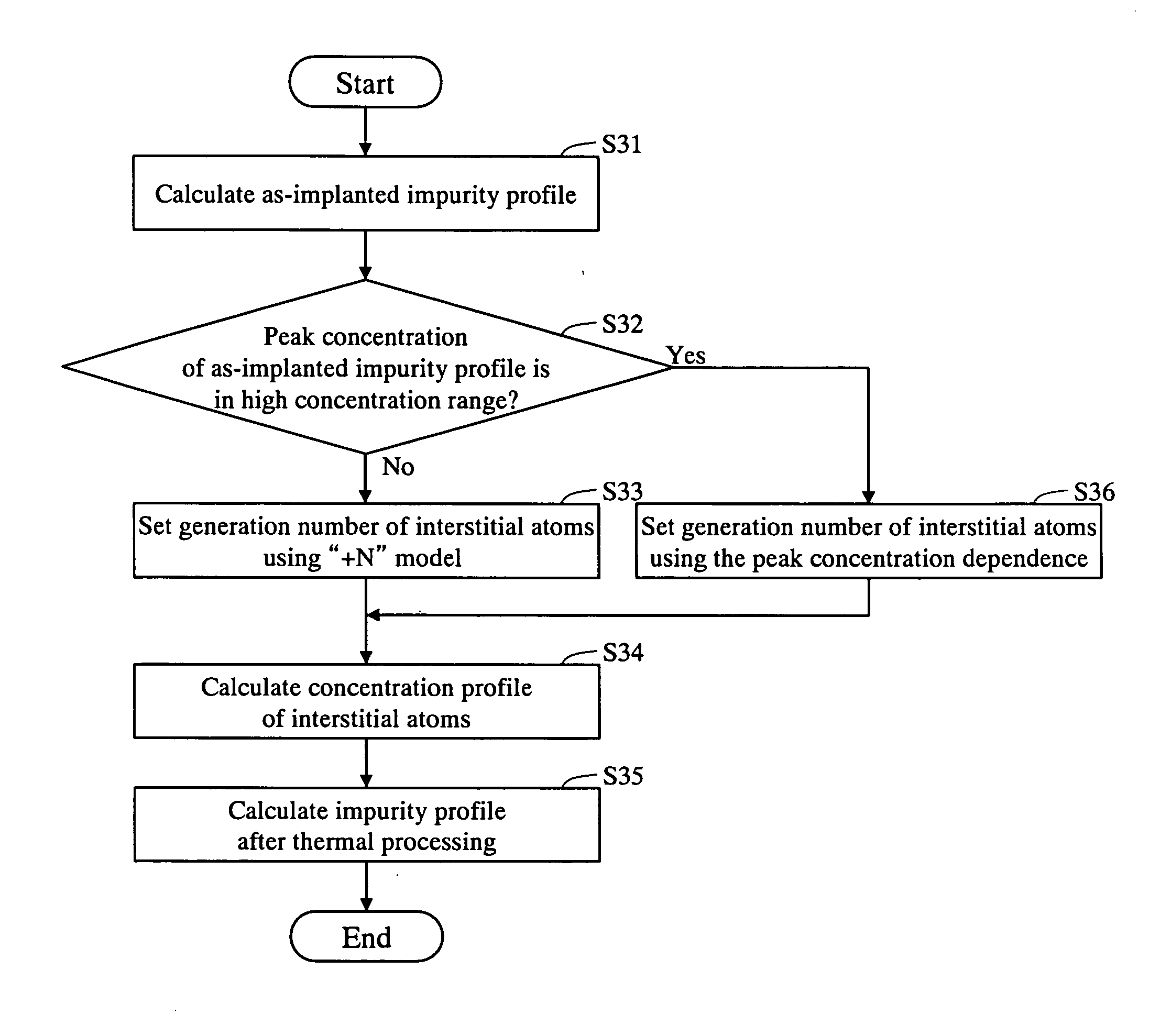
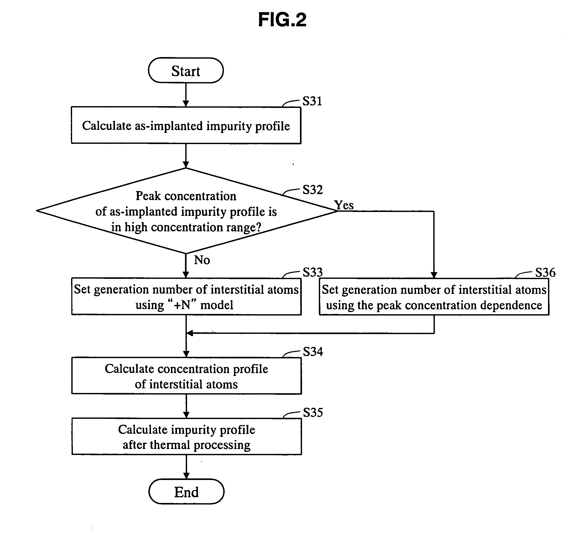
[0088]FIGS. 7A and 7B shows measured profile and predicted profile in case of implanting borondifluoride (BF2) in a silicon substrate with 50 keV implantation energy and 3.2×1013 cm−2 dose. FIG. 7A shows measured profile 71 and predicted profile 72 in as-implanted state. FIG. 7B shows measured profile 73 and predicted profile 74 in as annealed state. As the thermal processing in this example, the annealing is performed for 10 seconds at 850° C., and for 5 seconds at 1020° C. In this case, the peak concentration of as-implanted impurity profile is 5×1018 cm−3 and more, which is in the high concentration range, as shown in FIG. 7A. Accordingly, a value calculated based on the peak concentration dependence is set as the generation number of interstitial atoms.

[0089] According to FIG. 7B, it is understood that the predicted profile 74 corresponding to the measured profile 73 can be obtained.

example 2

[0090]FIGS. 8A and 8B shows measured profile and predicted profile in case of implanting boron (B) in a silicon substrate with 25 keV implantation energy and 1.2×1013 cm−2 dose. FIG. 8A shows measured profile 81 and predicted profile 82 in as-implanted state. FIG. 8B shows measured profile 83 and predicted profile 84 in as-annealed state. As the thermal processing in this example, the annealing is performed for 10 seconds at 850° C., and for 5 seconds at 1020° C. In this case, the peak concentration of as-implanted impurity profile is less than 5×1018 cm−3, which is the low concentration range, as shown in FIG. 8A. Accordingly, a value calculated based on the “+N” model (Equation 6) is set as the generation number of interstitial atoms.

[0091] According to FIG. 8B, it is understood that the predicted profile 84 corresponding to the measured profile 83 can be obtained.

example 3

[0092]FIGS. 9A and 9B shows measured profile and predicted profile in case of implanting boron (B) in a silicon substrate with 10 keV implantation energy and 1.6×1012 cm−2 dose, 100 keV implantation energy and 8.0×10l cm−2 dose, and 300 keV implantation energy and 4.0×1011 cm−2 dose, respectively. FIG. 9A shows measured profile 91 and predicted profile 92 in as-implanted state. FIG. 9B shows measured profile 93 and predicted profile 94 in as-annealed state. As the thermal processing in this example, the annealing is performed for 60 minutes at 850° C., and the oxidation processing is performed for 7.7 minutes at 900° C. (for forming 9 nm oxide film). In this case, the peak concentration of as-implanted impurity profile is less than 5×1018 cm−3, which is the low concentration range, as shown in FIG. 9A. Accordingly, a value calculated based on the “+N” model is set as the generation number of interstitial atoms.

[0093] According to FIG. 9B, it is understood that the predicted profile...


PUM


Abstract

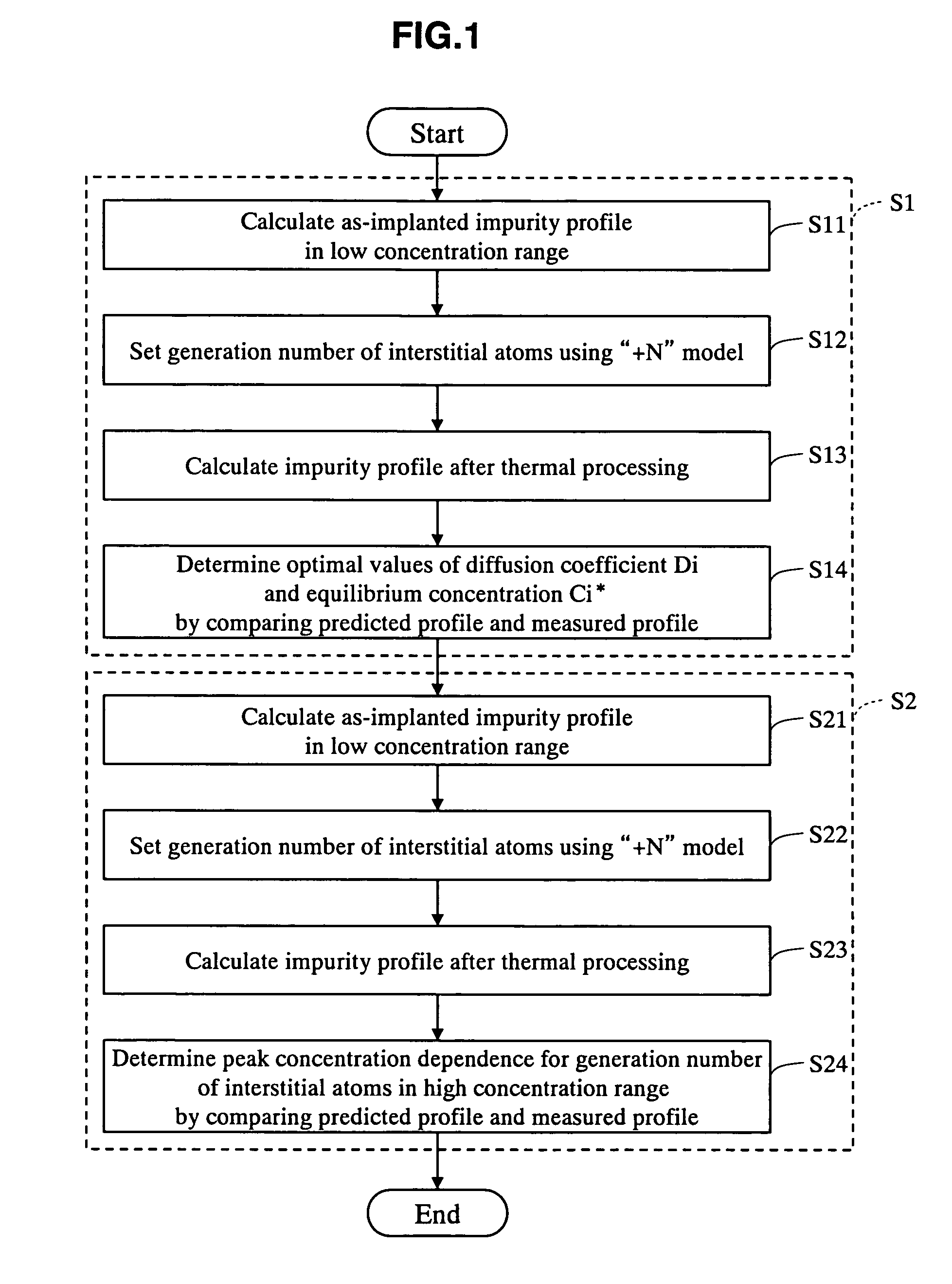
The as-implanted concentration profile of impurity atoms in the semiconductor substrate is calculated, and a number of interstitial atoms to be generated in the semiconductor substrate by one impurity atom implanted with the ion implantation is set based on a peak concentration of the calculated as-implanted concentration profile of impurity atoms. The concentration profile of interstitial atoms generated in the semiconductor substrate is calculated based on the calculated as-implanted concentration profile of impurity atoms and the set number of interstitial atoms, and the concentration profile of impurity atoms in the semiconductor after the thermal processing is calculated based on the calculated as-implanted concentration profile of impurity atoms and the calculated concentration profile of interstitial atoms.

Description

CROSS-REFERENCE TO RELATED APPLICATION [0001] The present application claims the benefit of patent application number 2005-197799, filed in Japan on Jul. 6, 2005, the subject matter of which is hereby incorporated herein by reference. FIELD OF THE INVENTION [0002] The present invention relates to impurity diffusion simulation methods, impurity diffusion simulation apparatus, and impurity diffusion simulation programs, and in particular, the invention relates to impurity diffusion simulation methods, impurity diffusion simulation apparatus, and impurity diffusion simulation programs, whereby concentration profile of impurity atoms after the thermal processing can be predicted in consideration for point defects generated at the implantation of impurity atoms into a silicon substrate with ion-implantation. DESCRIPTION OF RELATED ART [0003] In the process simulator, such as TSUPREM4 (Commercial Name) widely used, impurity diffusion equations considering interaction between impurity atom...

Claims


Application Information

Patent Timeline
Patent Type & Authority Applications(United States)
IPC IPC(8): H01L21/66H01L21/425
CPCG06F17/5009G06F2217/80G06F2217/16G06F30/20G06F2111/10G06F2119/08
Inventor TSUNO, MORIKAZU
Owner PANASONIC CORP
Learn More