Method for manufacturing semiconductor device

a semiconductor and manufacturing technology, applied in semiconductor devices, semiconductor/solid-state device details, electrical devices, etc., can solve the problems of resin boss carbonization and resin insulating resistance reduction, and achieve the effect of easy removal

Inactive Publication Date: 2007-02-01
138 EAST LCD ADVANCEMENTS LTD
View PDF9 Cites 35 Cited by
  • Summary
  • Abstract
  • Description
  • Claims
  • Application Information

AI Technical Summary

Benefits of technology

[0007] An advantage of some aspects of the invention is to improve contact characteristics of an electrical conducting layer and prevent migration.
[0009] According to the first aspect of the invention, the resin layer is fused, the surface is formed into a smooth curved surface, and the resin layer is cured and shrunk from such a shape. Therefore, a resin boss with a moderate rising section can be finally formed. Thereby, the electrical conducting layer is prevented from being exfoliated and disconnected, and the contact characteristics thereof can be improved.
[0012] According to the second aspect of the invention, the surface section of the resin layer is fused, the surface is formed into a smooth curved surface, and the resin layer is cured and shrunk from such a shape. Therefore, a resin boss with a moderate rising section can be finally formed. Thereby, the electrical conducting layer is prevented from being exfoliated and disconnected, and the contact characteristics thereof can be improved.
[0017] Thereby, even if carbonation of the resin boss is progressed by Ar gas and a carbonized layer (or plasma polymerization layer) is formed, the resin boss can be easily removed without leaving the carbonized layer or the like since the rising section of the resin boss is formed moderately. In particular, the carbonized layer or the like easily remains in the root section of the resin boss. However, according to the aspect of the invention, the carbonized layer or the like remaining in the root section of the resin boss can be easily removed.

Problems solved by technology

However, performing Ar contra-sputtering may lead to carbonization of the surface of the resin boss.
In result, insulating resistance of the resin may be decreased, which might cause migration.

Method used


Image

  • Method for manufacturing semiconductor device
  • Method for manufacturing semiconductor device
  • Method for manufacturing semiconductor device

Examples


Embodiment Construction

[0035] An embodiment of the invention will be described with reference to the drawings.

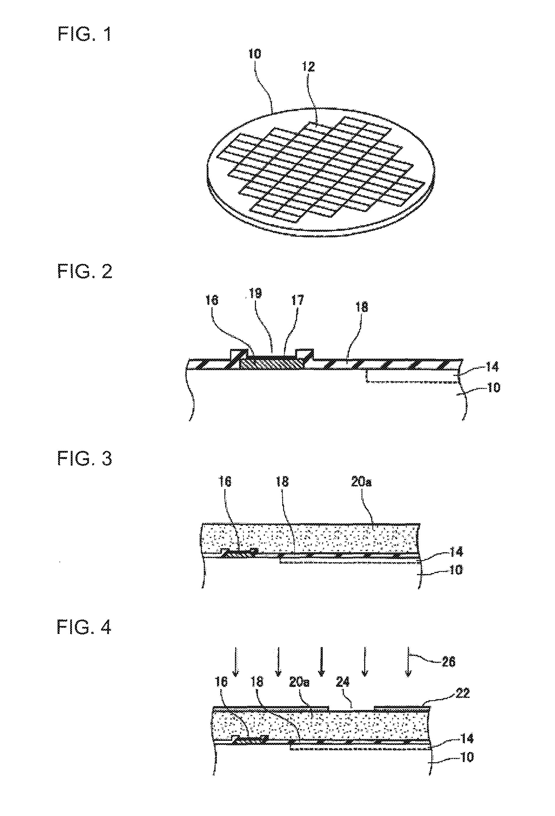
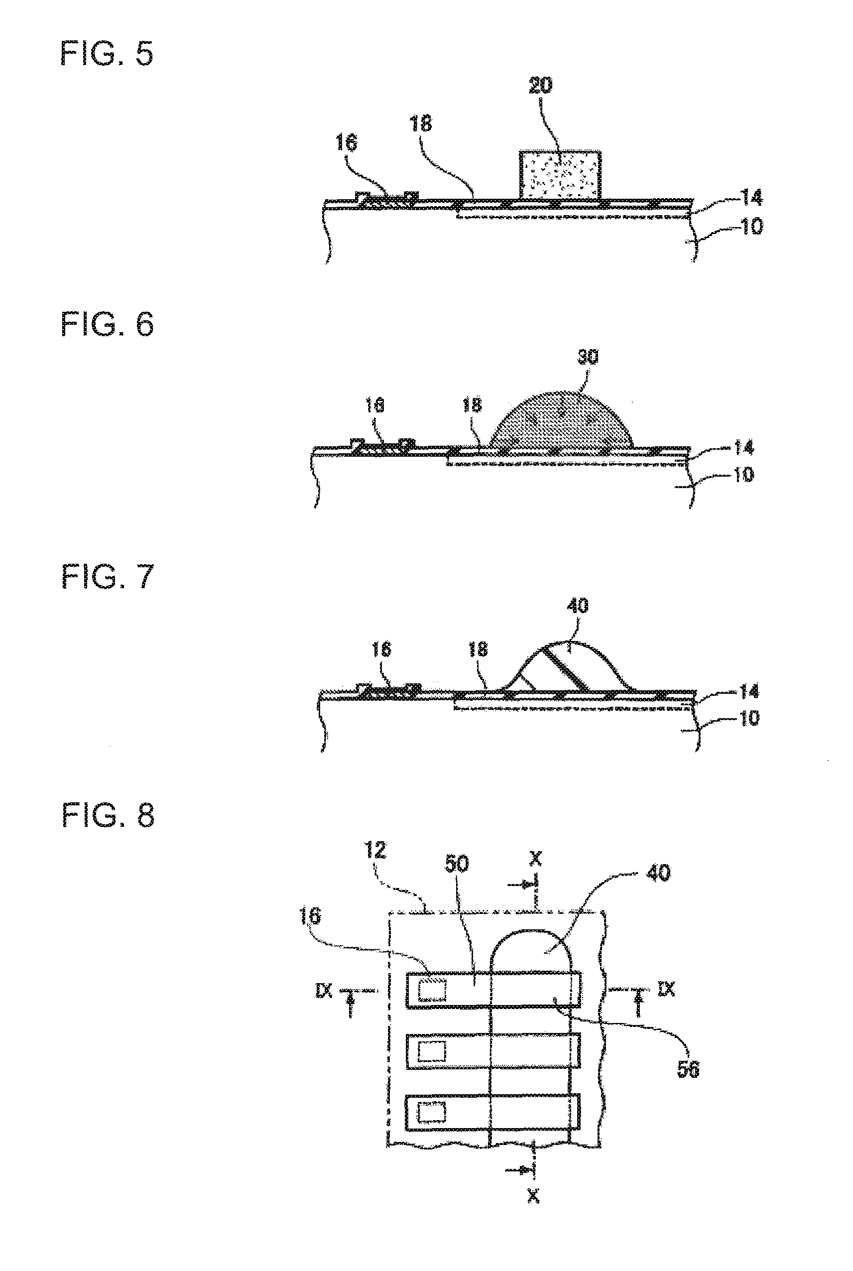
[0036] Method for manufacturing a semiconductor device FIG. 1 to FIG. 11 are drawings for explaining a method for manufacturing a semiconductor device according to the embodiment of the invention.

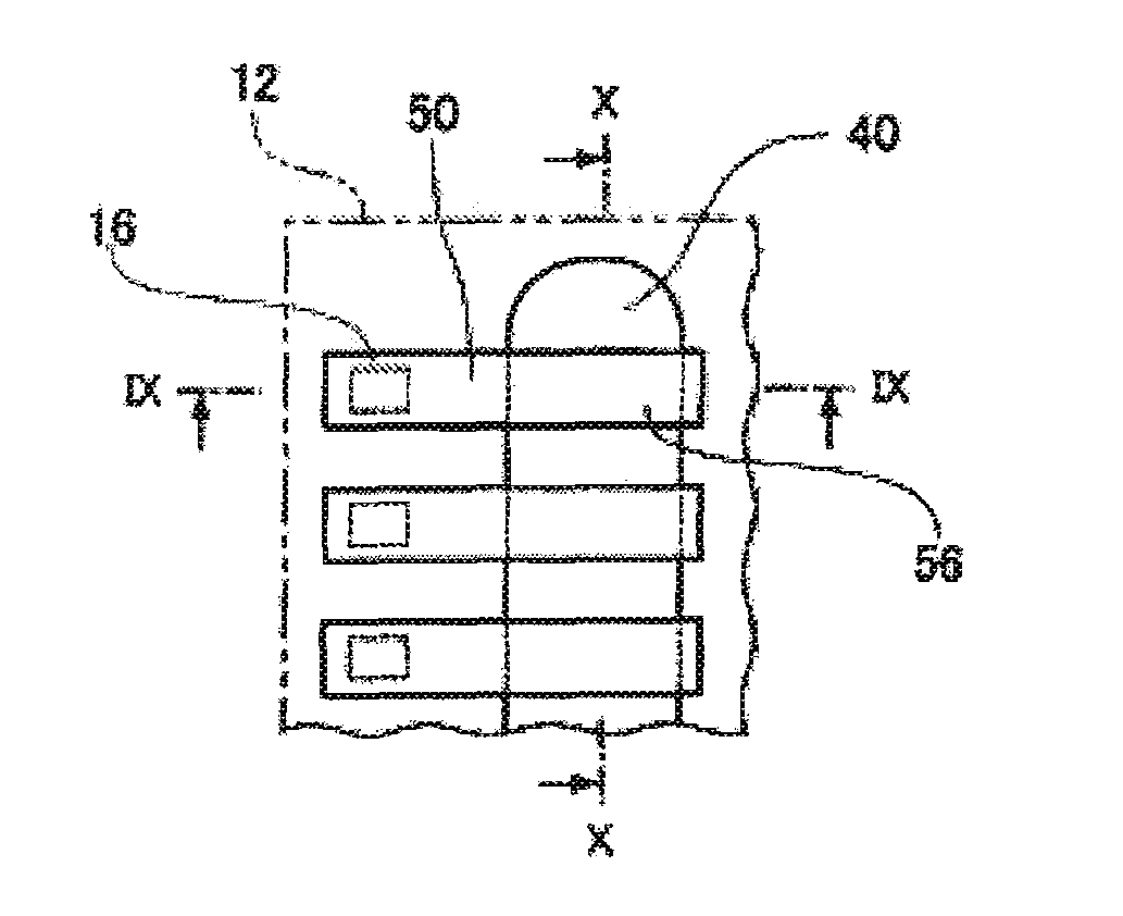
[0037] 1. First, as shown in FIG. 1 and FIG. 2, a semiconductor substrate 10 is prepared. The semiconductor substrate 10 is, for example, a semiconductor wafer (refer to FIG. 1). In this case, the semiconductor substrate 10 has a plurality of chip regions 12 to become semiconductor chips. An integrated circuit 14 is formed inside each chip region 12. That is, when the semiconductor substrate 10 is divided into the plurality of semiconductor chips, each semiconductor chip has each integrated circuit 14. The integrated circuit 14 includes at least active devices such as a transistor. The chip region 12 is in the shape of an orthogon (for example, rectangle) in the plan view. In each chip region 12, a plur...


PUM


Abstract

A method for manufacturing a semiconductor device, including: (a) forming an energy cured resin layer on a semiconductor substrate having an electrode pad and a passivation film; (b) fusing the resin layer without being cured and shrunk by a first energy supply processing; (c) forming a resin boss by curing and shrinking the resin layer after fusion by a second energy supply processing; and (d) forming an electrical conducting layer which is electrically connected to the electrode pad and passes through over the resin boss.

Description

[0001] The entire disclosure of Japanese Patent Application No. 2005-203487, filed Jul. 12, 2005 is expressly incorporated by reference herein. BACKGROUND OF THE INVENTION [0002] 1. Technical Field [0003] The present invention relates to a method for manufacturing a semiconductor device. [0004] 2. Related Art [0005] In order to improve electrical connection reliability, semiconductor devices using a resin core bump in which an electrical conducting layer is formed on a resin boss as an external terminal have been developed. According to such a semiconductor device, after the resin boss is formed on a semiconductor substrate, the electrical conducting layer is formed over from an electrode pad to the resin boss. In general, in a step of forming the electrical conducting layer, Ar contra-sputtering is performed to remove an oxide layer on the electrode pad. However, performing Ar contra-sputtering may lead to carbonization of the surface of the resin boss. In result, insulating resist...

Claims


Application Information

Patent Timeline
Patent Type & Authority Applications(United States)
IPC IPC(8): H01L21/47
CPCH01L23/525H01L24/11H01L2924/07802H01L2924/0001H01L2224/136H01L2224/1319H01L2924/01033H01L2924/01024H01L2924/01006H01L24/90H01L2224/13099H01L2224/90H01L2924/01013H01L2924/01015H01L2924/01018H01L2924/01029H01L2924/01046H01L2924/01078H01L2924/01079H01L2924/01082H01L2924/14H01L24/13H01L2924/01005H01L2924/00014H01L2924/00H01L24/02H01L24/05H01L2224/05001H01L2224/05008H01L2224/05022H01L2224/05124H01L2224/05548H01L2224/05624H01L2224/05644H01L2224/05647H01L2224/05655H01L2224/05664H01L2224/05671H01L2224/13008H01L2924/12044H01L2224/02
Inventor YAMASAKI, YASUOTANAKA, SHUICHIHASHIMOTO, NOBUAKI
Owner 138 EAST LCD ADVANCEMENTS LTD
Why Eureka
Try Eureka