Injection molded microoptics

a micro-optics and injection molding technology, applied in the field of high-efficiency waferscale micro-electronic process, can solve the problems of difficult to achieve long focal length high radius of curvature and high refractive index micro-lens arrays, poor control of the fill-factor of the photodiodes in the array comprising the pixel plane, and poor control of the fill-factor of the photodiodes. , to achieve the effect of high optical design,

Active Publication Date: 2007-02-08
IBM CORP
View PDF8 Cites 77 Cited by
  • Summary
  • Abstract
  • Description
  • Claims
  • Application Information

AI Technical Summary

Benefits of technology

[0011] Another object of the present invention is to provide processes for the wafer-scale fabrication of microoptic devices, which can be integrated into semiconductor structures, such as a color-imaging device for digital cameras. A further object of this invention is to extend this fabrication process to include liquid crystal materials which may be formed into active lens arrays with electronically variable focal length and depth of focus. In accord with another object of the present invention, there is provided a manufacturing method and microelectronic fabrication process sequence which minimizes the number and task-times of the operational unit-process steps required in the reduces of semiconductor arrays for color imaging devices. Production cost minimization is consistent with this latter object of the present invention.
[0013] Attachment of semiconductor chips to carriers, modules or packages using controlled collapse chip connection (“C4”) technology has proven to provide superior electrical performance parameters, such as minimizing parasitics, mutual inductance, controlled impedance, and noise reduction. It is an object of the present invention to enable the concurrent use of the injection-molding apparatus for the hybrid use of solders for C4 joining of chips to substrates and for optical polymers or glasses for forming and attaching microoptic elements.

Problems solved by technology

Coupled with the resist's index of refraction, the resulting microlens array will have a focal length and light-collection properties which may depart from desired optimum performance, including poor control of the fill-factor of the photodiodes in an array comprising the pixel plane.
Optical design of the lens shape and refractive index is extremely limited by the necessity to use photoimageable materials with restricted thermal reflow characteristics.
It is difficult to achieve long focal length high radius of curvature and high refractive index microlens arrays in a single array-plane using conventional microlens forming and fabrication processes.
Topographical variations caused by the process of integrating color filters into the semiconductor, as shown in FIG. 1B, are a common problem in the Prior Art and typically require additional processing steps for adding a planarizing layer.

Method used


Image

  • Injection molded microoptics
  • Injection molded microoptics
  • Injection molded microoptics

Examples


Embodiment Construction

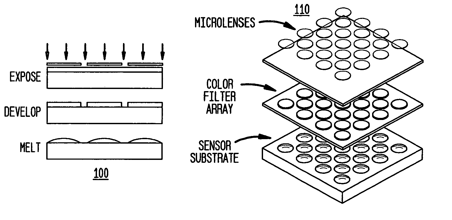
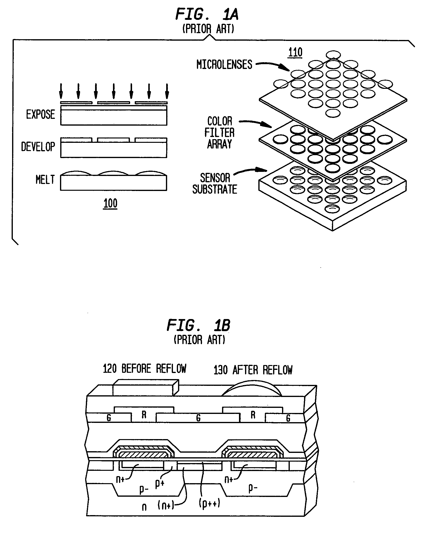
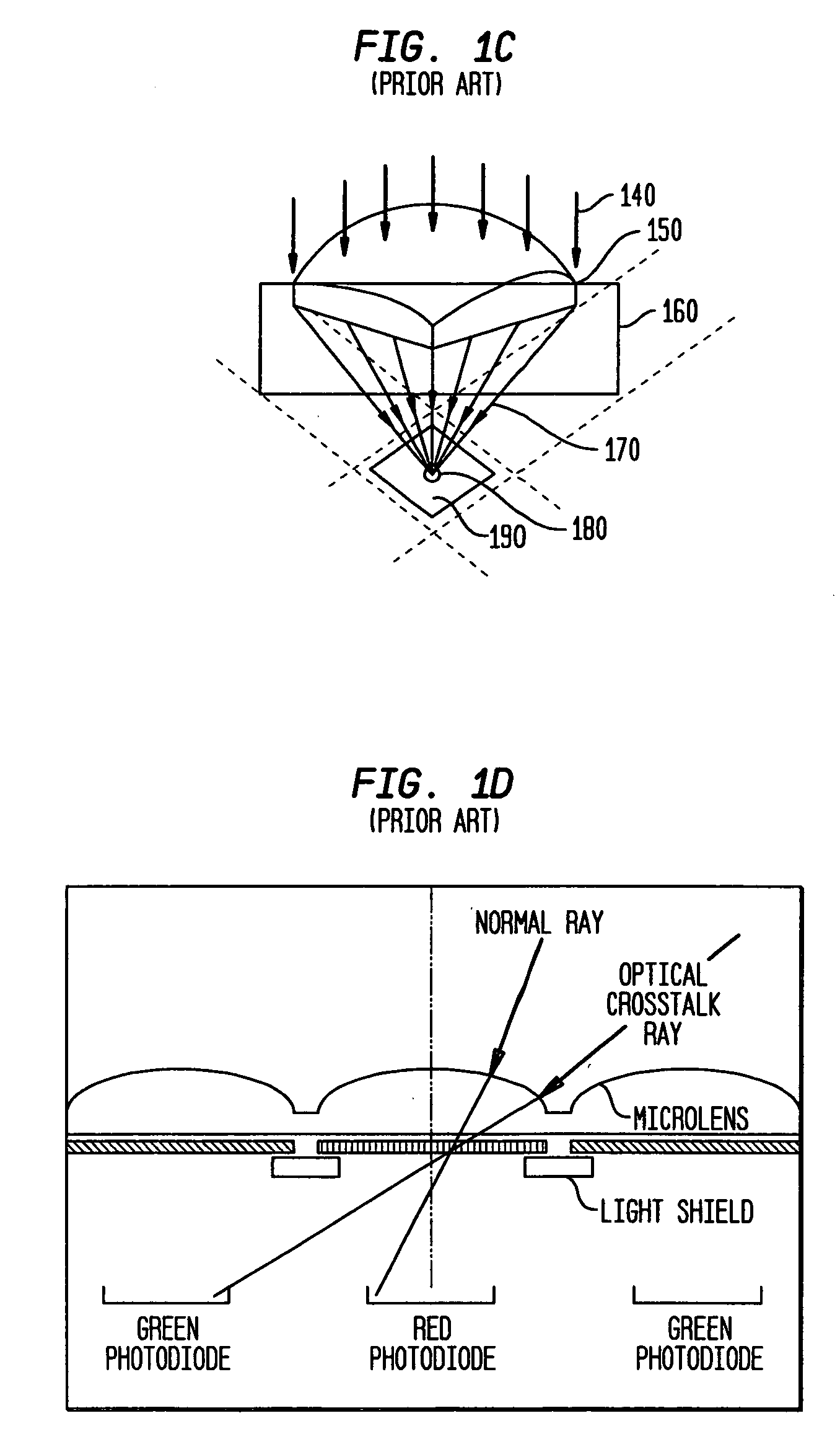
[0029] The present invention teaches an apparatus and method for the formation of planar arrays of microlenses and / or optical waveguides and photonic devices which may comprise, inter alia, optical bus I / O and memory structures in advanced future computer backplanes, image-formation layers on CMOS or CCD solid-state color imagers, matrix arrays of lenses on flat panel displays, and other fields of applications for microoptic elements.

[0030] Unlike conventional art, aspherics, anamorphics, cylindrical lenticular and ellipsoidal microoptic surface designs may be realized with the present invention to provide the long focal lengths required for semiconductor color imaging devices or for VCSEL (vertical cavity surface emitting laser) couplers, particularly those used in parallel optical links including applications such as InfiniBand channels for computers and storage devices. Employment of high refractive index materials, such as polymers, or glasses, or liquid crystal materials, with...


PUM

PropertyMeasurementUnit
diameteraaaaaaaaaa
pressuresaaaaaaaaaa
divergence angleaaaaaaaaaa

Abstract

A wafer-scale apparatus and method is described for the automation of forming, aligning and attaching two-dimensional arrays of microoptic elements on semiconductor and other image display devices, backplanes, optoelectronic boards, and integrated optical systems. In an ordered fabrication sequence, a mold plate comprised of optically designed cavities is formed by reactive ion etching or alternative processes, optionally coated with a release material layer and filled with optically specified materials by an automated fluid-injection and defect-inspection subsystem. Optical alignment fiducials guide the disclosed transfer and attachment processes to achieve specified tolerances between the microoptic elements and corresponding optoelectronic devices and circuits. The present invention applies to spectral filters, waveguides, fiber-optic mode-transformers, diffraction gratings, refractive lenses, diffractive lens / Fresnel zone plates, reflectors, and to combinations of elements and devices, including microelectromechanical systems (MEMS) and liquid crystal device (LCD) matrices for adaptive, tunable elements. Preparation of interfacial layer properties and attachment process embodiments are taught.

Description

CROSS REFERENCE TO RELATED APPLICATION [0001] This application is related to copending application Ser. No. ______ (Attorney Docket YOR920050131US1), filed herewith, for “Injection Molded Microlenses For Optical Interconnects,” the disclosure of which is herein incorporated by reference in its entirety.BACKGROUND OF THE INVENTION [0002] 1. Field of the Invention [0003] The present invention relates to a highly efficient wafer-scale microelectronic process for the fabrication of spectral filters, microoptics, optical waveguide arrays and their aligned attachment to optoelectronic semiconductor imaging devices, integrated photonic devices, image displays, optical fiber interconnection, optical backplanes, memory devices, and spectrochemical or biomedical analysis devices. [0004] 2. Background Art [0005] Synthetic reconstruction of color images in solid-state analog or digital video cameras is conventionally performed through a combination of an array of optical microlens and spectral ...

Claims


Application Information

Patent Timeline
Patent Type & Authority Applications(United States)
IPC IPC(8): B29D11/00B29C35/08B29C45/00
CPCB29D11/00365B29D11/00461B82Y30/00G02B3/0018H01L33/58H01L27/14627H01L27/14685H01L31/02327G02B3/0056B29D11/00307G02F1/29G02F1/137
Inventor JACOBOWITZ, LAWRENCEBUCHWALTER, STEPHEN L.DECUSATIS, CASIMERGRUBER, PETER A.SHIH, DA-YUAN
Owner IBM CORP
Why Eureka
Try Eureka