Capacitor for incorporation in wiring board, wiring board, method of manufacturing wiring board, and ceramic chip for embedment

a technology of capacitors and wiring boards, applied in the direction of fixed capacitor details, fixed capacitors, printed circuit non-printed electric components association, etc., can solve the problems of reducing the layout freedom affecting the layout of other electronic components, and increasing the number of processes. disadvantages, etc., to achieve high reliability, high adhesive strength, and the effect of thermal stress on the buildup layer

Inactive Publication Date: 2007-02-08
NGK SPARK PLUG CO LTD
View PDF17 Cites 81 Cited by
  • Summary
  • Abstract
  • Description
  • Claims
  • Application Information

AI Technical Summary

Benefits of technology

[0013] In the case of the above-cited JP-A-2005-39217 and JP-A-2005-39243, the obverse surface of the ceramic chip is exposed on the obverse surface of the core portion, while the reverse surface of the ceramic chip is exposed on the reverse surface of the core portion. For this reason, a portion of the interlayer insulating layer constituting the buildup layer is formed on not only the board core but also the ceramic chip. However, in the case of the above-described conventional wiring board for IC chip mounting, it is difficult to ensure high adhesive strength between the interlayer insulating layer

Problems solved by technology

In conjunction with this trend, there are cases where noise is superimposed on the power source wiring and the like, possibly resulting in erroneous operation.
With the above-described technique, however, since it is necessary to mount the capacitor separately after the completion of the wiring board, the number of processes disadvantageously increases.
In addition, there is a need to secure in advance a region where the capacitor is mounted on the wiring board, so that the freedom of the layout of other electronic components declines.
Furthermore, because the region where the capacitor is mounted on the wiring board is restricted by other wiring and the like, the wiring distance between the capacitor and the semiconductor chip becomes long, so that

Method used


Image

  • Capacitor for incorporation in wiring board, wiring board, method of manufacturing wiring board, and ceramic chip for embedment
  • Capacitor for incorporation in wiring board, wiring board, method of manufacturing wiring board, and ceramic chip for embedment
  • Capacitor for incorporation in wiring board, wiring board, method of manufacturing wiring board, and ceramic chip for embedment

Examples


first embodiment

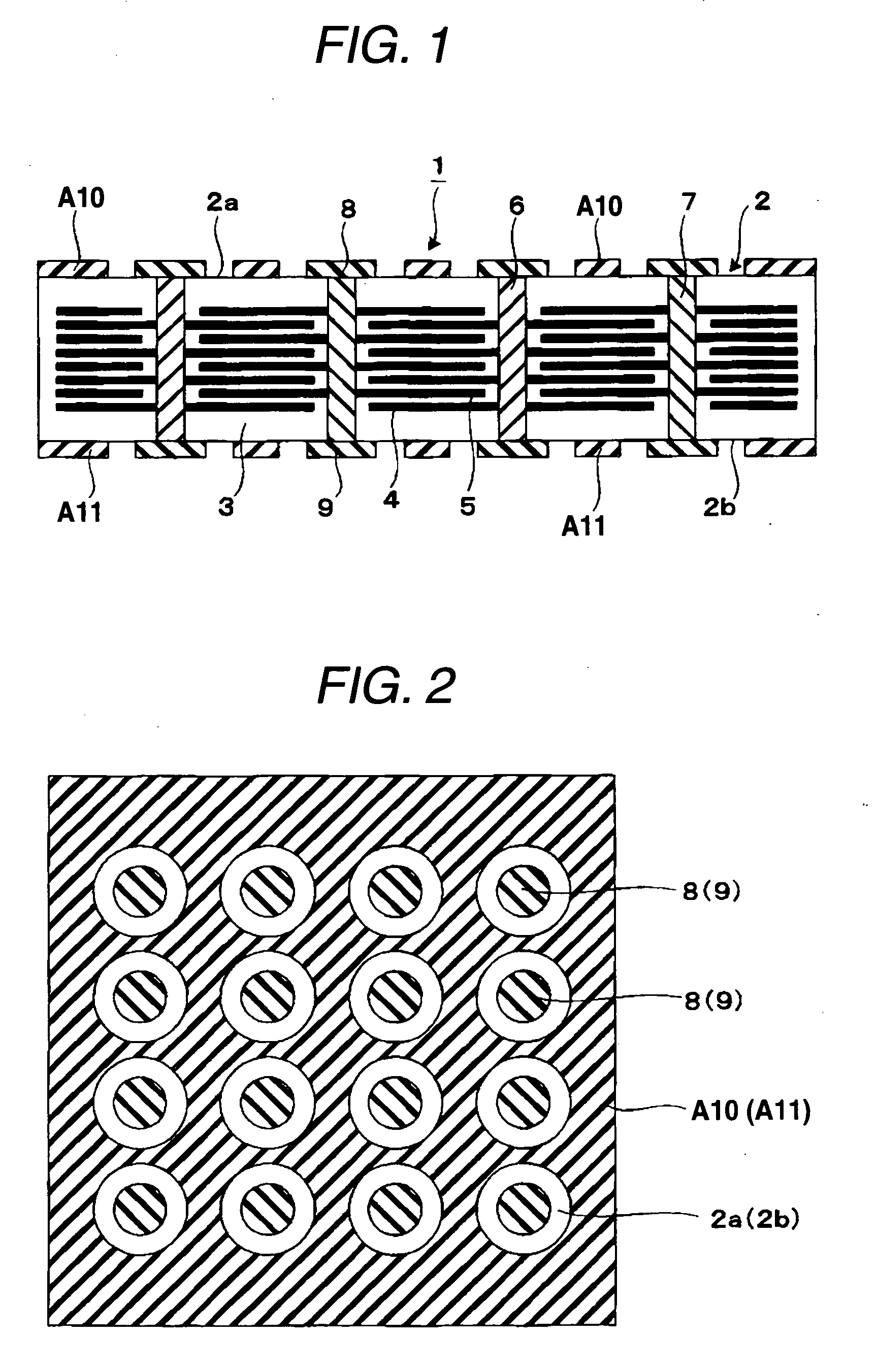
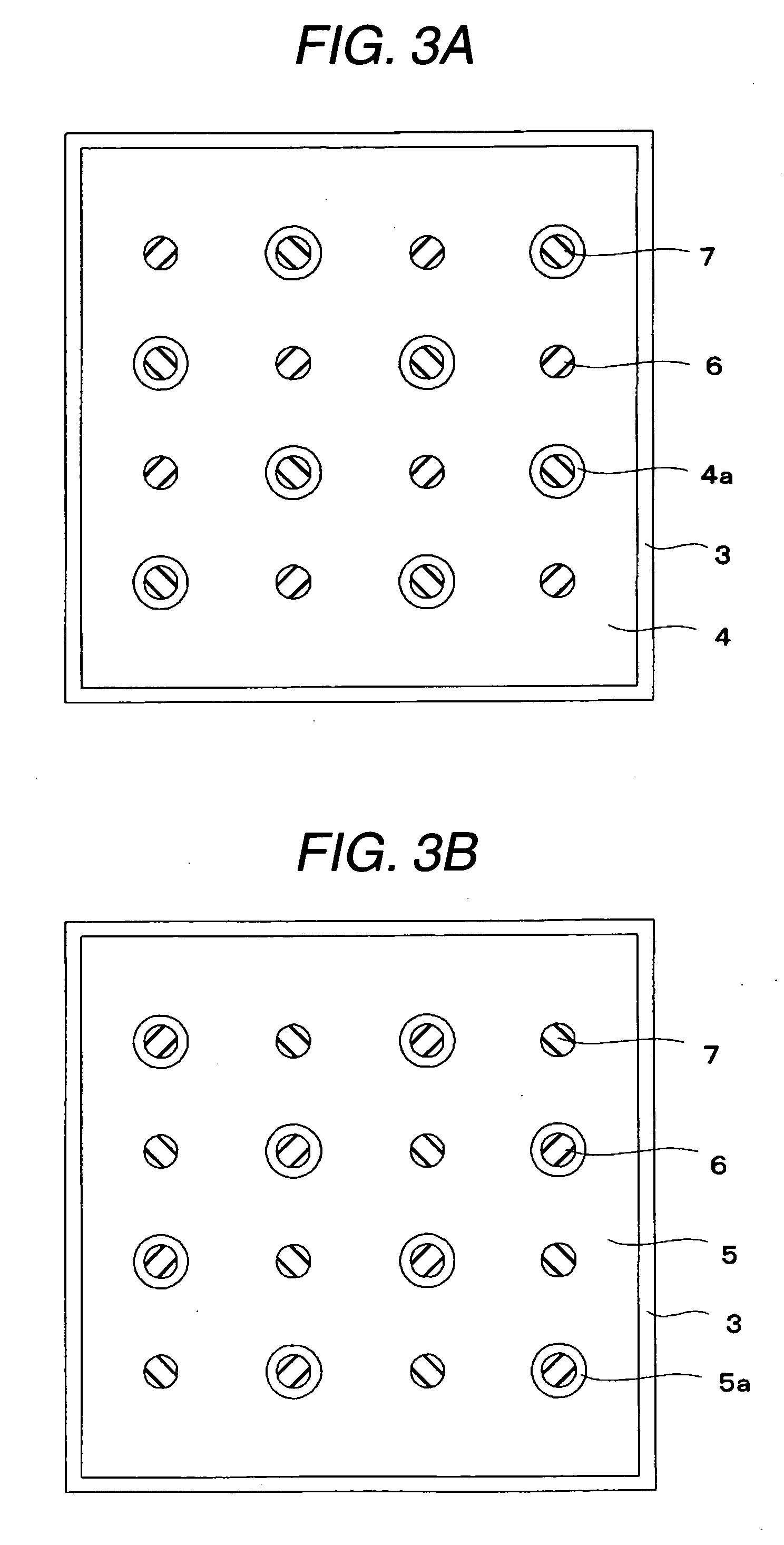
[0143] Referring now to the drawings, a description will be given of a first embodiment of the invention. FIG. 1 is a schematic vertical cross-sectional view of a capacitor for incorporation in a wiring board in accordance with this embodiment. FIG. 2 is a schematic plan view of the capacitor for incorporation in a wiring board in accordance with this embodiment. FIGS. 3A and 3B are schematic horizontal cross-sectional views of the capacitor for incorporation in a wiring board in accordance with this embodiment.

[0144] A capacitor 1 for incorporation in a wiring board (hereafter, simply the “capacitor”) shown in FIGS. 1 to 3B is a laminated capacitor formed in the shape of a rectangular parallelepiped. The capacitor 1 has a capacitor body2 constituting the core of the capacitor 1. The capacitor body 2 is comprised of a plurality of ceramic layers 3 (dielectric layers) laminated in the vertical direction, as well as pluralities of inner electrode layers 4 and 5 each disposed between ...

second embodiment

[0184] Hereafter, a description will be given of a second embodiment of the invention with reference to the drawings. In this embodiment, a description will be given of an example in which the area of the surface(s) of the outer electrode(s) 8 is set to be not less than 45% and not more than 90% of the area of the first main surface 2a, and the area of the surface(s) of the outer electrode(s) 9 is set to be not less than 45% and not more than 90% of the area of the second main surface 2b. It should be noted that identical members to the members described in the first embodiment will be denoted by the same reference numerals, and the contents which overlap with those described in the first embodiment will be omitted except for those described below. FIG. 7 is a schematic vertical cross-sectional view of the capacitor for incorporation in a wiring board in accordance with this embodiment. FIG. 8 is a schematic plan view of the capacitor for incorporation in a wiring board in accordanc...

third embodiment

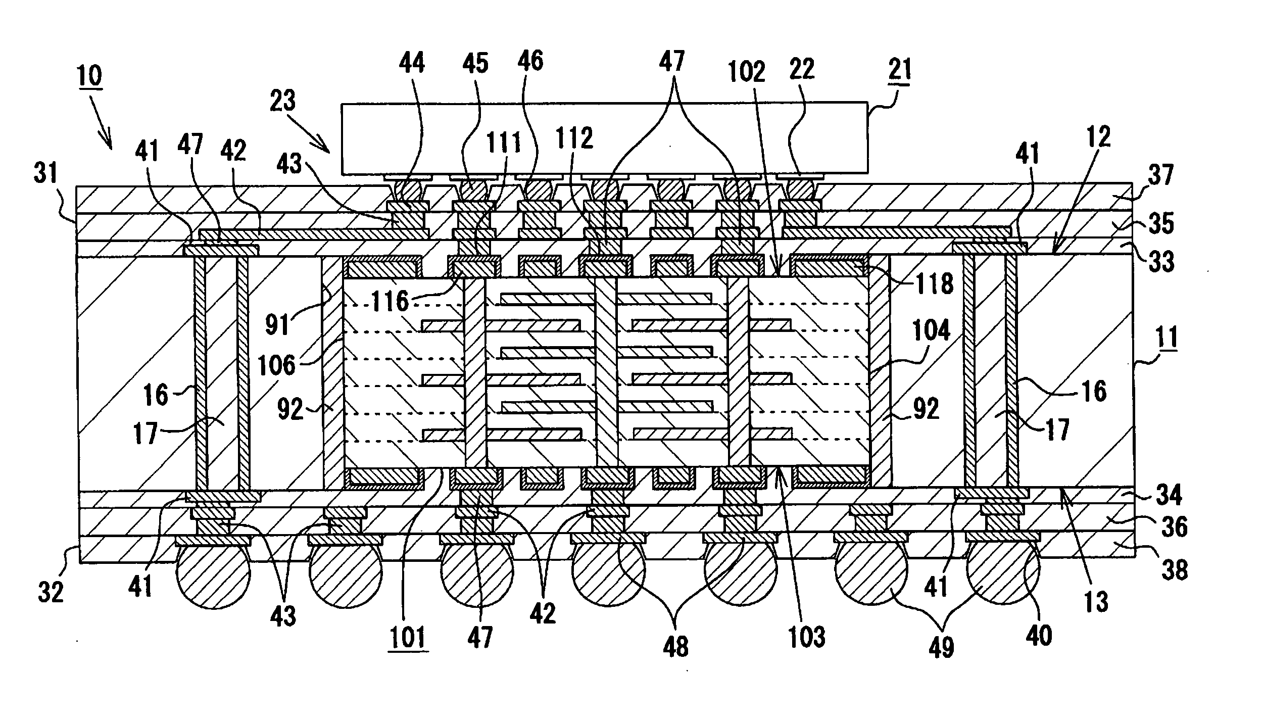
[0191] Referring now to the drawings, a detailed description will be given of a third embodiment of the wiring board in accordance with the invention.

[0192] As shown in FIG. 9, a wiring board 10 in accordance with this embodiment is comprised of a substantially rectangular plate-shaped board core 11 which is a wiring board for mounting on an IC chip and is formed of glass epoxy; a buildup layer 31 formed on an upper surface 12 (core main surface) of the board core 11; and a buildup layer 32 formed on a lower surface 13 of the board core 11. Through hole conductors 16 are formed at a plurality of portions in the board core 11. These through hole conductors 16 connect and conduct the upper surface 12 side and the lower surface 13 side of the board core 11. It should be noted that the interior of each through hole conductor 16 is filled with a closure body 17 such as an epoxy resin. Further, conductor layers 41 formed of copper are respectively pattern-formed on the upper surface 12 a...


PUM


Abstract

A capacitor comprising: a capacitor body including a plurality of laminated dielectric layers, a plurality of inner electrode layers which are respectively disposed between mutually adjacent ones of the dielectric layers, a first main surface located in a laminated direction of the dielectric layers, and a second main surface opposite to the first main surface; a first outer electrode formed on the first main surface of the capacitor body and electrically connected to the inner electrode layers; a second outer electrode formed on the second main surface of the capacitor body and electrically connected to the inner electrode layers; a first dummy electrode formed on the first main surface of the capacitor body; and a second dummy electrode formed on the second main surface of the capacitor body.

Description

BACKGROUND OF THE INVENTION [0001] 1. Field of the Invention [0002] The present invention relates to a capacitor for incorporation in a wiring board and a wiring board having the same. Furthermore, the present invention concerns a wiring board having a structure in which a ceramic chip for embedment is embedded in an accommodating hole portion of a board core, and a buildup layer is formed by being laminated on its surface, as well as a method of manufacturing the same, and a ceramic chip for embedment. [0003] 2. Description of the Related Art [0004] In recent years, the speed of the operation of semiconductor chips is becoming increasingly higher due to advancement in the integrated circuit technology. In conjunction with this trend, there are cases where noise is superimposed on the power source wiring and the like, possibly resulting in erroneous operation. Accordingly, a capacitor is mounted on an upper surface or a lower surface of a wiring board on which the semiconductor chip...

Claims


Application Information

Patent Timeline
IPC IPC(8): H01G4/06
CPCH01G4/232H01L2224/16235H01L23/49822H01L2224/16225H01L2924/01078H01L2924/01079H01L2924/09701H01L2924/15311H05K1/0231H05K1/112H05K1/185H05K3/4602H05K2201/096H05K2201/09781H05K2201/10674H05K2201/10712H01L2924/01019H01G4/30H01L2224/05568H01L2224/05573H01L2924/00014H01L2924/3511H01L2224/05599
Inventor YAMAMOTO, HIROSHISEKI, TOSHITAKEYURI, SHINJIMURAMATSU, MASAKISATO, MOTOHIKOHAYASHI, KAZUHIROOTSUKA, JUNSATO, MANABU
Owner NGK SPARK PLUG CO LTD
Why Eureka
Try Eureka