Nucleation layer deposition on semiconductor process equipment parts

a technology of process equipment and nucleation layer, which is applied in the field of manufacturing of integrated circuit chips, can solve the problems of reducing the overall conductivity of the layer, affecting the production efficiency of semiconductor products, so as to achieve good adhesion to the surface, reduce the effect of flaking and strong adhesion

Inactive Publication Date: 2007-02-08
STMICROELECTRONICS SRL
View PDF3 Cites 16 Cited by
  • Summary
  • Abstract
  • Description
  • Claims
  • Application Information

AI Technical Summary

Benefits of technology

[0010] Having a large number of nucleation sites provides many locations where the oxide atoms may redeposit themselves and begin to grow a new layer on the inside surface of the bell jar. In addition, once the new layer begins to form at one or more nucleation sites, additional oxide atoms, will cling onto the growing layer at each nucleation site, thus forming a growing layer on the interior of the wall of the pre-clean chamber. The nucleation layer of the oxide results in growing an oxide layer on the inside wall of the plasma chamber, which can continue for

Problems solved by technology

This will reduce the overall conductivity of the layer or, in a worst case scenario cause defects in the formation of the integrated circuit components.
Unfortunately, such deposit

Method used


Image

  • Nucleation layer deposition on semiconductor process equipment parts
  • Nucleation layer deposition on semiconductor process equipment parts
  • Nucleation layer deposition on semiconductor process equipment parts

Examples


Embodiment Construction

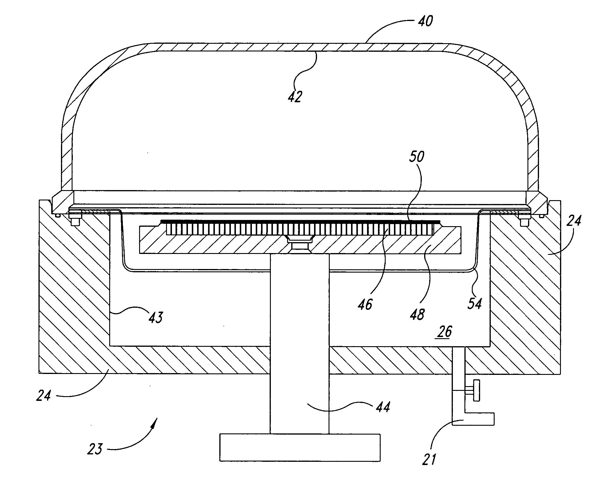
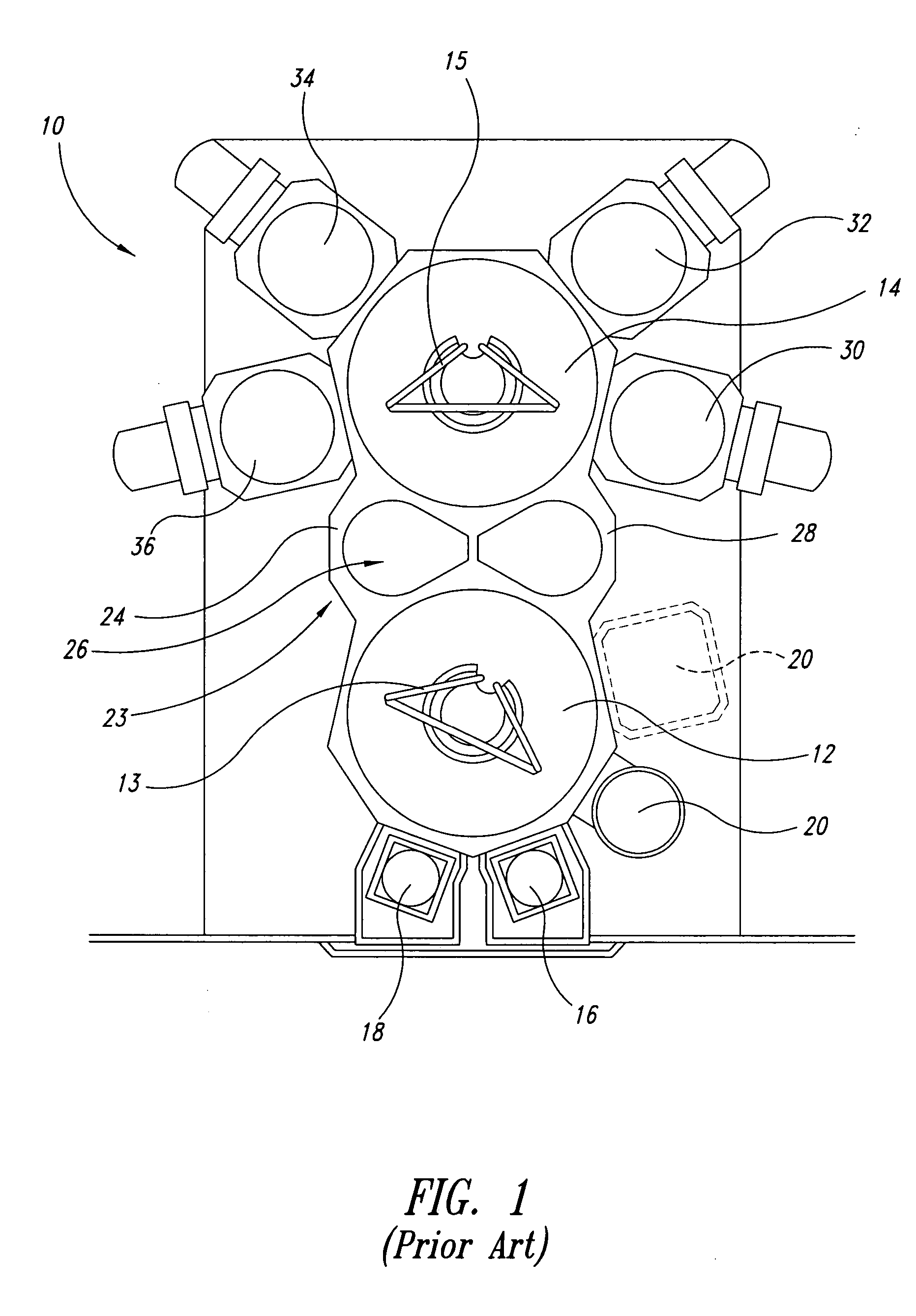
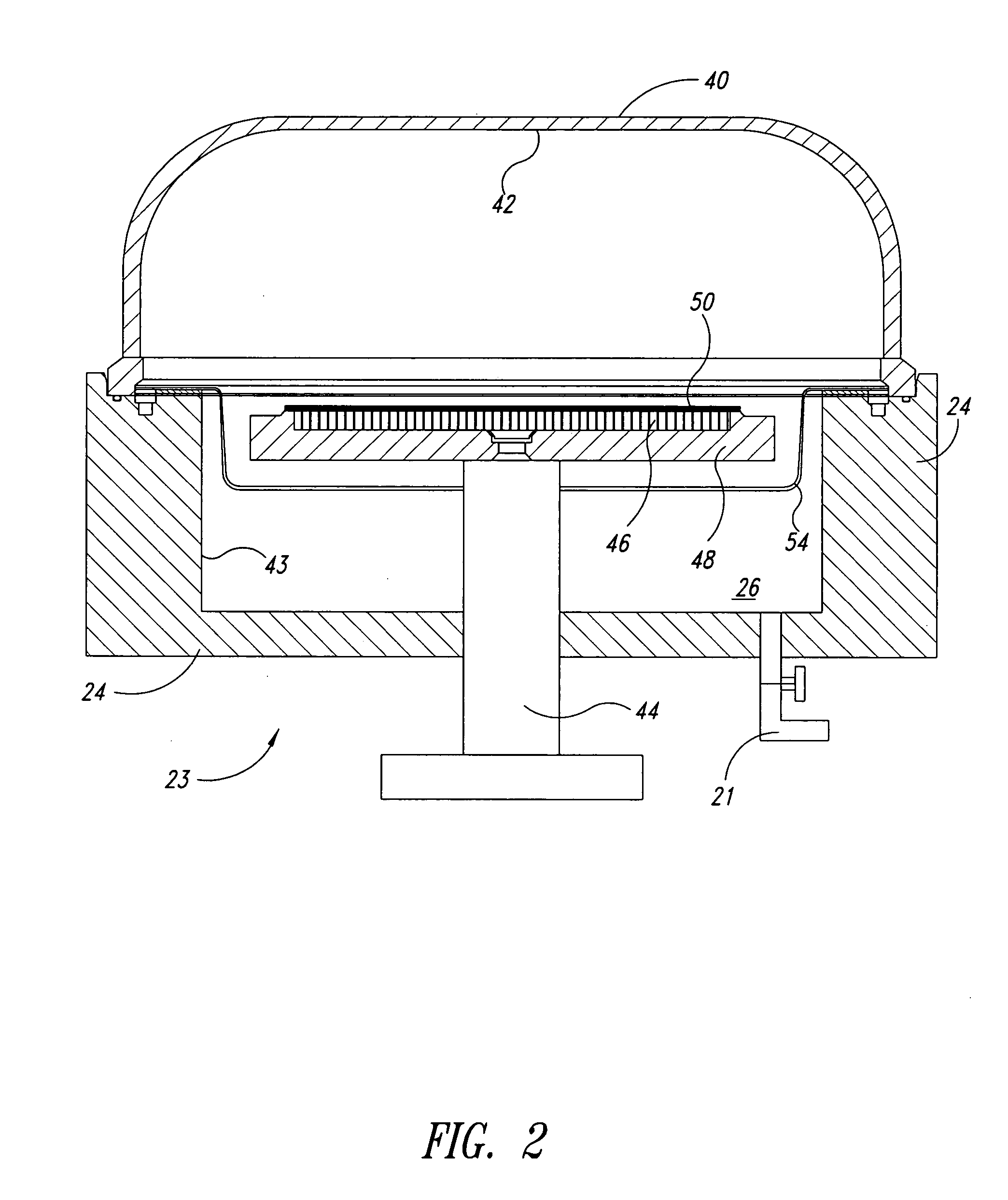
[0021]FIG. 1 is a top side view of one example of a well-known semiconductor processing facility in which the invention may be used. The processing facility 10 includes a number of chambers all of which are well known in the art, as is their operation. The facility 10 is provided as one example of the facility in which the invention may find use and, of course it may find use in other structures and facilities besides the one shown here. The example of FIG. 1 is based on the ENDURA layout, made by Applied Materials. A semiconductor processing facility 10 is available on the open market, which is well known in the art.

[0022] This particular semiconductor processing facility includes a first wafer handling chamber 12 and a second wafer handling chamber 14. The first wafer handling chamber 12 is usually used as a buffer chamber in which semiconductor wafers are prepared for further steps in the fabrication process. A robot arm 13 picks up the wafer and moves it from station to station...


PUM

PropertyMeasurementUnit
Temperatureaaaaaaaaaa
Areaaaaaaaaaaa
Timeaaaaaaaaaa

Abstract

A plasma chamber is provided having an upper insulating member as a lid of the plasma chamber. The lid of the plasma chamber, usually in the form of a bell jar, has an inside surface which will be exposed to the interior of the plasma chamber. A nucleation layer is affixed to the inside surface of the insulating member. The nucleation layer is selected to be a material which will enhance the growth on itself of the particular material being etched within the process chamber. For example, if the pre-clean chamber is being used to etch oxides, the nucleation layer is selected to be of a type which will create a large number of nucleation sites for the growth of an oxide layer on the interior wall of the bell jar. Each nucleation site becomes the starting point for the adherence of the etched oxide atoms onto the wall of the bell jar. Wafers pre-cleaned in such a chamber have a lower defect density. Further, longer times are permitted between cleaning and replacing components in the pre-clean chamber.

Description

BACKGROUND OF THE INVENTION [0001] 1. Field of the Invention [0002] This invention is related to the manufacturing of semiconductor products, and more particularly to a machine for the manufacture of integrated circuit chips. [0003] 2. Description of the Related Art [0004] The processing of integrated circuit chips occurs in a number of different steps. The steps are often carried out in different etch chambers, others are carried out in furnaces, while others of which are deposition or implantation chambers. The semiconductor wafer frequently moves from one chamber to another as part of the integrated circuit fabrication process. [0005] One of the process chambers frequently used as the wafer is moved from station to station is a pre-clean chamber. The pre-clean chamber is used to clean or etch material from a substrate to prepare it for the next stage by various techniques, including sputter etching, plasma etching, or the like. The etching may, for example remove portions of a to...

Claims


Application Information

Patent Timeline
IPC IPC(8): H01L21/44
CPCC23C16/4404H01J37/32871H01J37/32623H01J37/32477
Inventor SIDHWA, ARDESHIR
Owner STMICROELECTRONICS SRL
Why Eureka
Try Eureka