Fabrication method for fabricating a semiconductor structure and semiconductor structure

a technology of semiconductor structure and fabrication method, which is applied in the direction of semiconductor devices, basic electric elements, electrical apparatus, etc., can solve the problems of leakage current problems below the threshold voltage, retention time problems, and affect the controllability of setting, so as to maximize the maximum current, improve the process control of the divots, and improve the effect of the maximum electric field strength variation

Inactive Publication Date: 2007-02-15
INFINEON TECH AG
View PDF16 Cites 4 Cited by
  • Summary
  • Abstract
  • Description
  • Claims
  • Application Information

AI Technical Summary

Benefits of technology

[0007] According to the invention, only the oxide removal above the active zone influences the depth of the STI divots. The edge rounding is essentially dominated, therefore, by the depth to which the STI oxide is pulled back prior to the hydrogen process and by the temperature of the subsequent H2 heat treatment process. A better process control of the divots can thereby be achieved.
[0008] In an advantageous manner, according to the invention, it is possible to avoid an edge of the active region and therefore an enclosing of such an edge of an active zone by a later gate structure. It furthermore becomes possible to maximize the maximum current in the ON state of a MOS transistor device that is later to be provided there. Consequently, both the radius of curvature at the top side of the active region and the electrically effective divot depth can be set since the process stops in a self-aligning manner, as it were, once the state of lowest energy has been attained.
[0009] The two aspects have a positive effect on the variation of the maximum electric field strength over the chip and thereby improve the Vt control and accordingly the retention time distribution in the case of a semiconductor memory device fabricated therefrom, for example. In experiments, the additional H2 step additionally resulted in an increase in the threshold voltage Vt by approximately 120 mV in comparison with a conventional method without edge rounding for the same ON current.

Problems solved by technology

An STI divot at an edge of an active zone of a transistor device impairs the controllability of setting the threshold voltage since field strength effects that are difficult to control occur at the edge.
In the case of customary MOS transistor devices, the enclosing of the edge of the transistor device by the gate oxide and the gate conductor is a factor which reduces the threshold voltage at the edge of the transistor device below the threshold voltage in the central region of the channel and thus creates leakage current problems below the threshold voltage.
Particularly in the case of transistor devices of DRAM memory devices, excessively low threshold voltages may result in retention time problems on account of leakage currents below the threshold voltage.

Method used


Image

  • Fabrication method for fabricating a semiconductor structure and semiconductor structure
  • Fabrication method for fabricating a semiconductor structure and semiconductor structure
  • Fabrication method for fabricating a semiconductor structure and semiconductor structure

Examples


first embodiment

[0020] FIGS. 1A-E show schematic illustrations of successive method stages of a fabrication method of a semiconductor structure as the present invention.

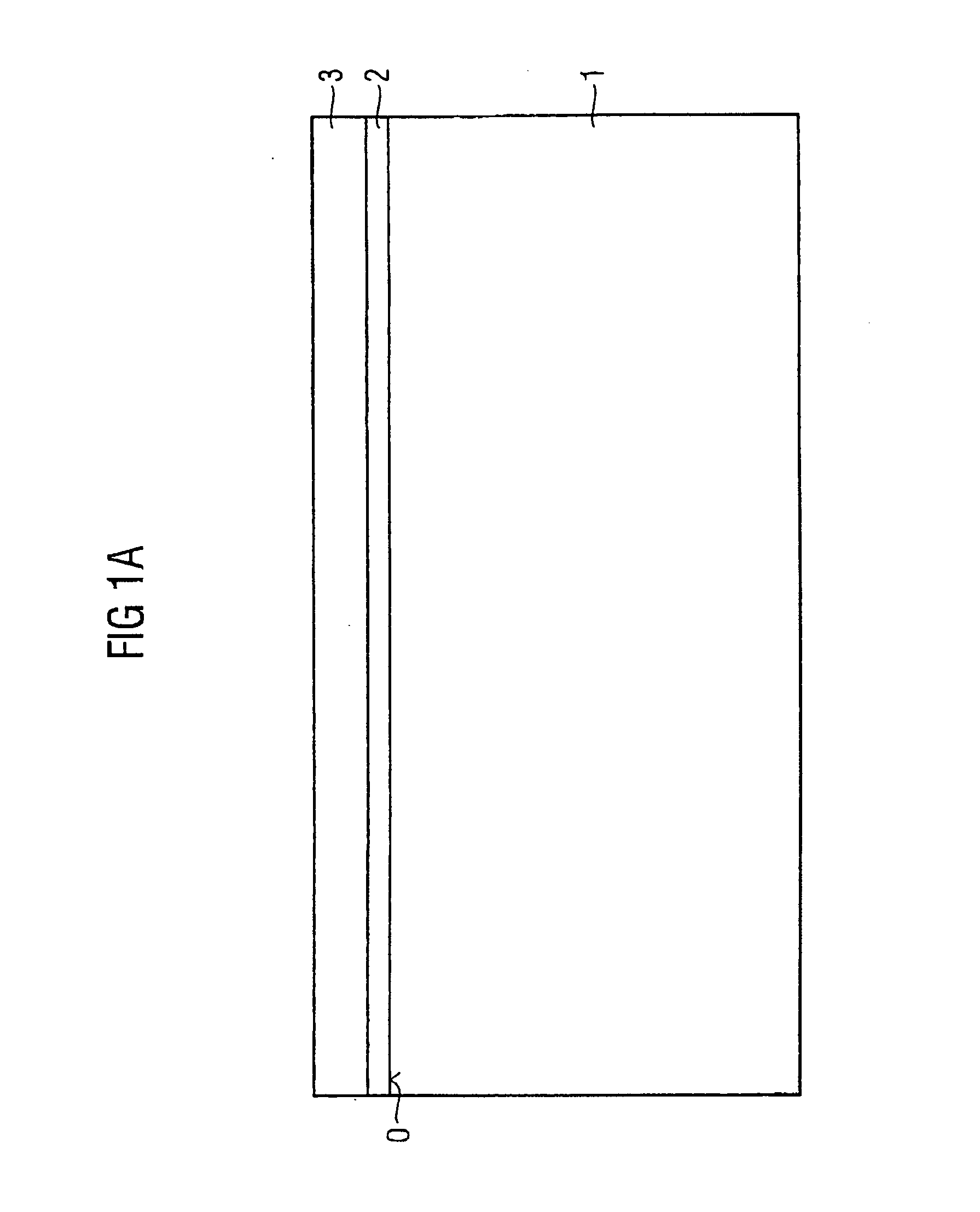
[0021] In FIG. 1A, reference symbol 1 designates a silicon semiconductor substrate, to the top side O of which are applied a pad oxide layer 2 and, above the latter, a pad nitride layer 3.

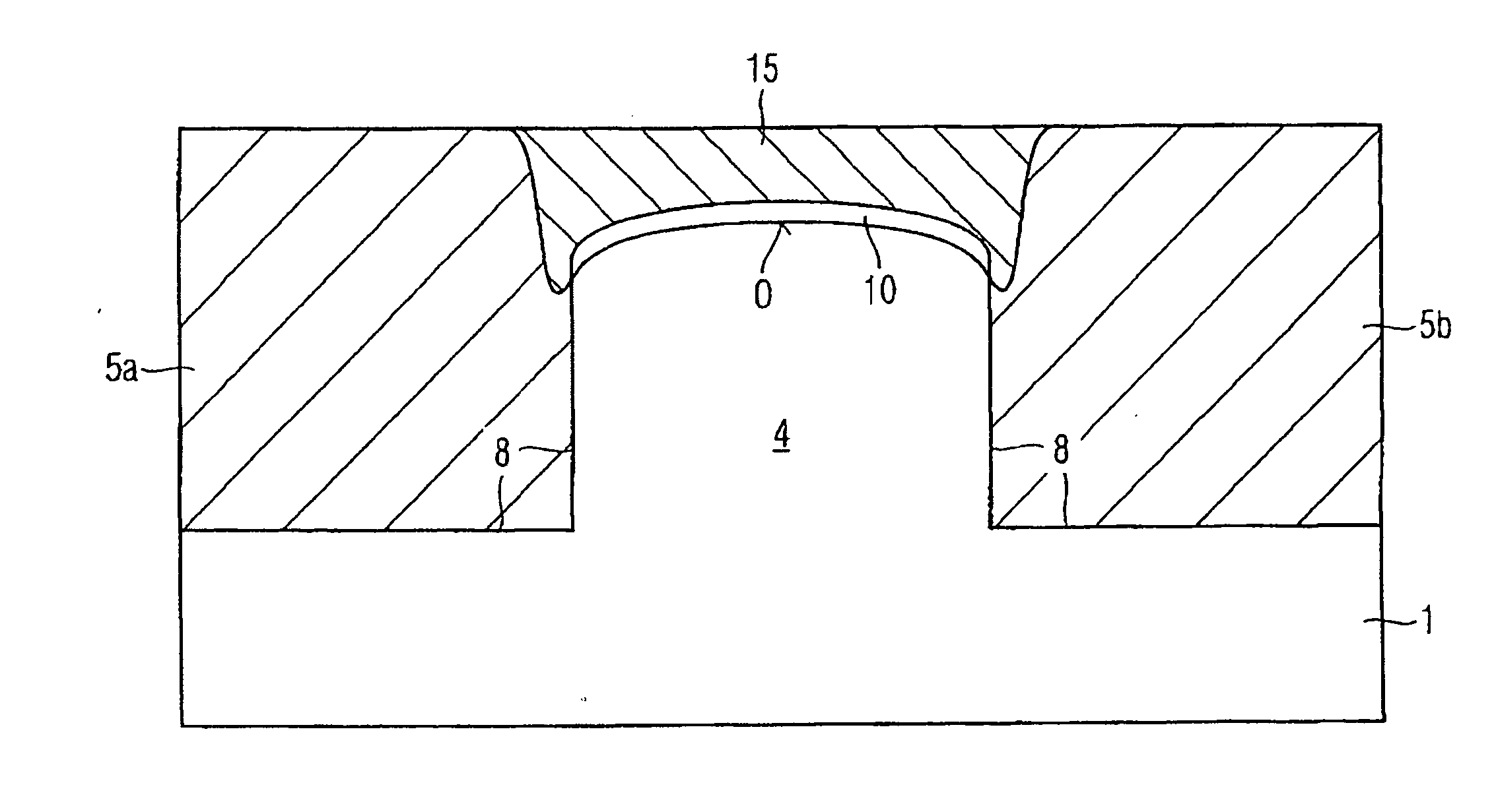
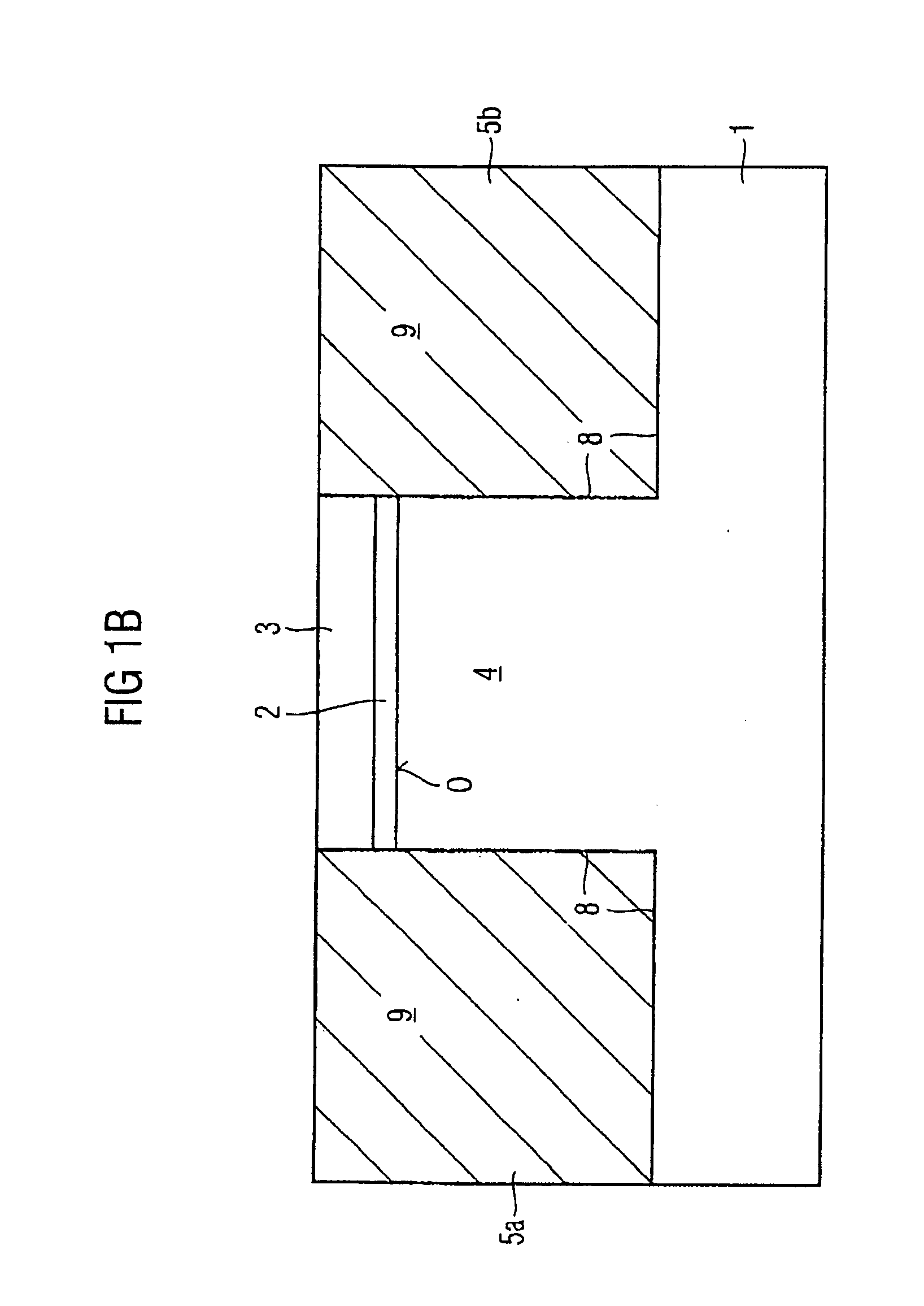
[0022] Referring further to FIG. 1B, by means of a method known per se, mask openings (not illustrated) are formed in the pad oxide layer 2 and pad nitride layer 3 and STI trenches 5a, 5b are subsequently etched into the semiconductor substrate 1 with the aid of said mask openings. The walls of the STI trenches 5a, 5b are then provided with a thermal oxide layer 8, and, finally, the STI trenches 5a, 5b are filled with an insulating silicon oxide filling 9 and planarized as far as the top side of the pad nitride layer 3 by means of a CMP process (chemical mechanical polishing). This leads to the structure shown in FIG. 1b, reference symbol 4 repres...

second embodiment

[0030] The second embodiment in accordance with FIGS. 2A to C involves an RCAT transistor device (RCAT=Recessed Channel Array Transistor), in which a U-shaped channel runs through a silicon semiconductor substrate 1′ along a trench 20 with a gate dielectric 10′ and a gate conductor 15′, as shown in FIG. 2A. The reference symbols 7 and 8 designate a source and drain zone, respectively.

[0031]FIG. 2A represents a longitudinal section through an RCAT transistor device of this type, whereas FIGS. 2B and 2C illustrate a cross section along the sectional line X in FIG. 2A.

[0032] As can be gathered from FIG. 2B, the active region 4′ is bounded on both sides by a respective STI trench 5a′, 5b′ in the transverse direction. During the fabrication of the trench 20, divots D1′, D2′ form at the edges K′ of the active region 4′.

[0033] Following the process state shown in FIG. 2B, the H termination of the top side O′ in a vaporous or liquid HF solution as already described in connection with the ...


PUM


Abstract

In a method for fabricating a semiconductor structure a semiconductor substrate comprising an active region with an uncovered top side is provided, at least one STI trench adjoining the active region is formed, and an STI divot is formed in the insulating filling. The at least one STI trench comprises an insulating filling extending to above the top side of the active region and the divot adjoins the active region and uncovers an edge of the uncovered top side of the active region. A hydrogen termination of the uncovered top side of the active region is formed and a heat treatment in a hydrogen atmosphere is carried out in order to form a rounding from the edge of the active region in such a way that the top side of the active region continuously merges into the STI divot.

Description

BACKGROUND OF THE INVENTION [0001] The present invention relates to a method for fabricating a semiconductor structure and a semiconductor structure. [0002] An STI divot at an edge of an active zone of a transistor device impairs the controllability of setting the threshold voltage since field strength effects that are difficult to control occur at the edge. On the other hand, a wraparound of the planar gate area by use of STI divots is useful if the transistor's on current that can be achieved is desired to be increased. The depth of such divots and thus the magnitude of this disadvantageous effect have been influenced hitherto by a plurality of successive wet etching steps. A certain edge rounding of the active zone arose in this case as a result of the pull-back of the pad nitride layer, the oxidation of the active zones and possible sacrificial oxide oxidations. [0003] In the case of customary MOS transistor devices, the enclosing of the edge of the transistor device by the gate...

Claims


Application Information

Patent Timeline
Patent Type & Authority Applications(United States)
IPC IPC(8): H01L21/8238
CPCH01L21/76224H01L29/1037H01L27/10873H10B12/05
Inventor BIRNER, ALBERTWEBER, ANDREASWEIS, ROLF
Owner INFINEON TECH AG
Why Eureka
Try Eureka