

Semiconductor device and its manufacturing method
a technology of semiconductor devices and manufacturing methods, applied in the direction of semiconductor devices, basic electric elements, electrical equipment, etc., can solve the problems of reduced electrical conductivity, reduced electrical conductivity, and increased wiring resistance owing to miniaturization of wiring, so as to reduce the electrical conductivity of the surface scattering of electrons and the effect of suppressing the scattering of electrons
- Summary
- Abstract
- Description
- Claims
- Application Information
AI Technical Summary
Benefits of technology
Problems solved by technology
Method used
Image

Examples
first embodiment
[0046] A first embodiment of the present invention is directed to a semiconductor device which comprises a wiring with small surface roughness formed on a smoothed barrier metal as an underlying layer for a Cu wiring, and its manufacturing method.
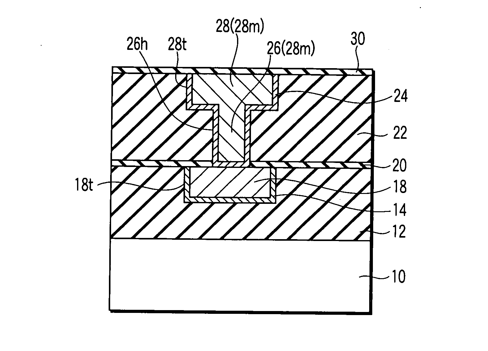
[0047]FIG. 8 is a sectional view of the semiconductor device to explain a Cu multilevel wiring. To simplify the description, Cu wirings 18, 28 of two layers are shown. According to the embodiment, a first interlevel insulator 12 is formed over an active element (not shown) such as a metal oxide semiconductor field effect transistor (MOSFET) formed on a semiconductor substrate 10 , e.g., a silicon substrate, and planarized its surface by, e.g., chemical mechanical polishing (CMP). A first wiring groove 18t is formed in the first interlevel insulator 12, and the first wiring 18 is formed therein via a first barrier metal 14 . A first diffusion preventive film 20 is formed on an entire surface of the first wiring 18 and the first interlevel i...
second embodiment
[0054] A second embodiment of the present invention is directed to a semiconductor device which comprises a wiring with small surface roughness formed on a smoothed surface of a low dielectric constant insulator used as an interlevel insulator, and its manufacturing method.
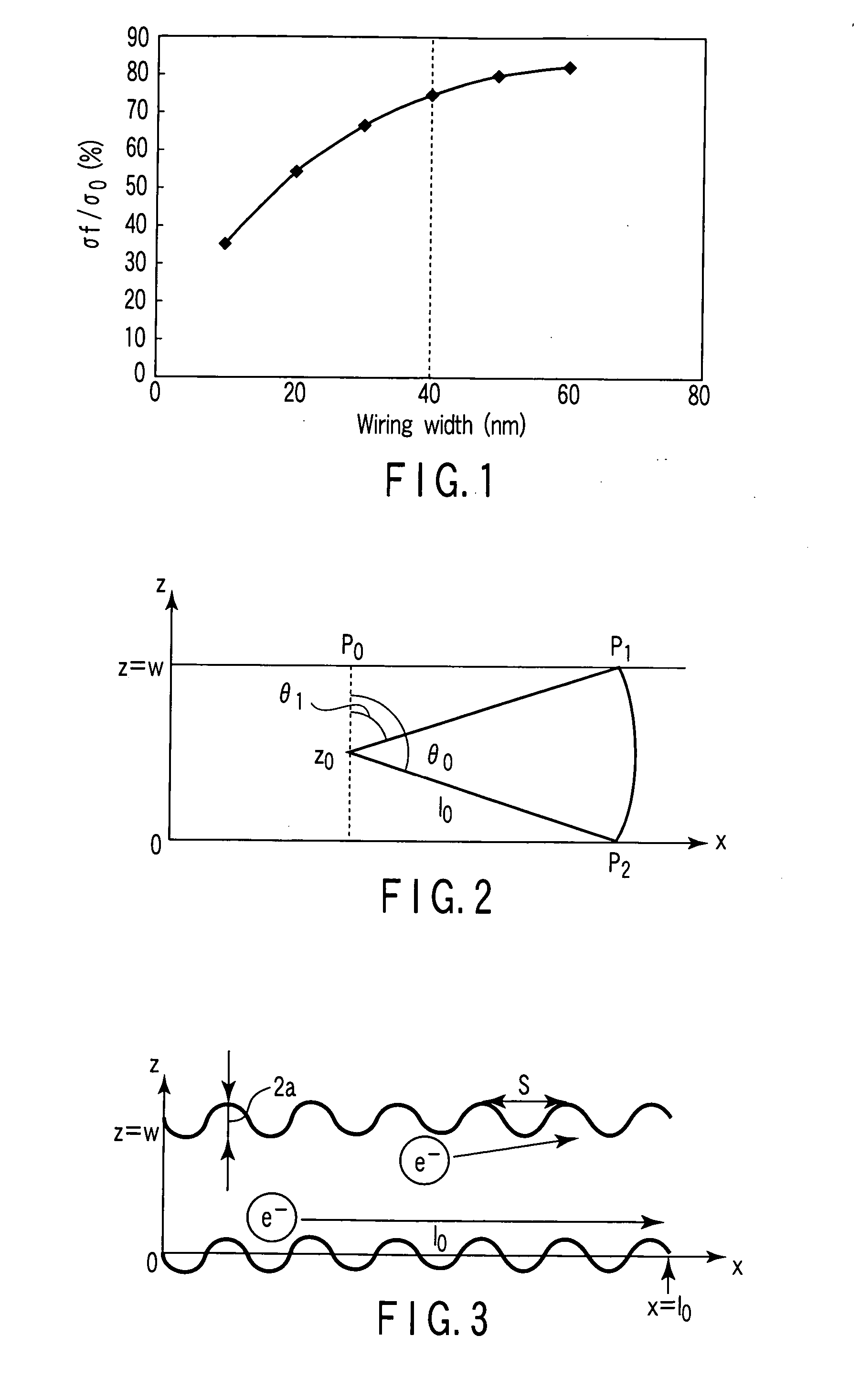
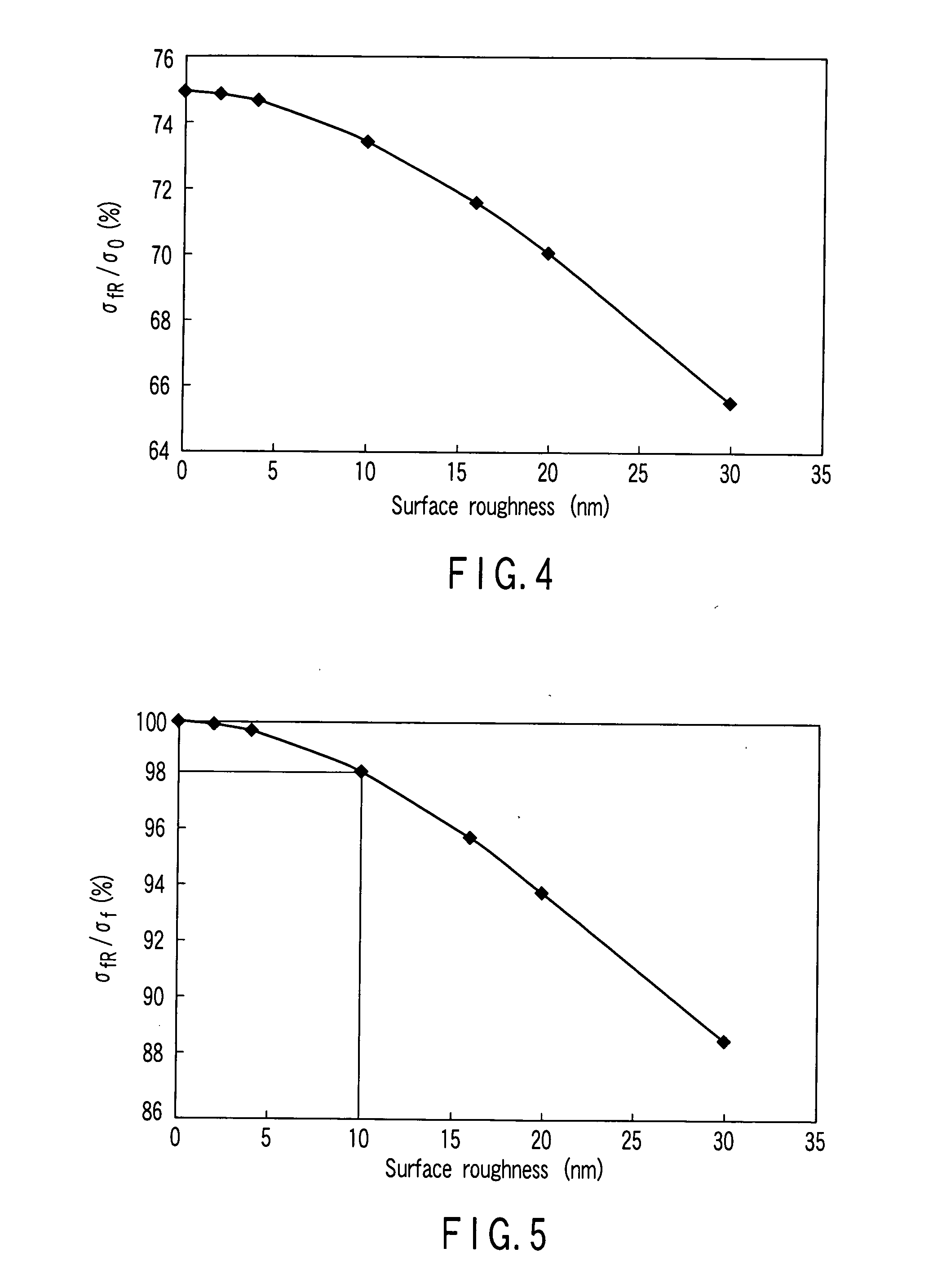
[0055] When a feature size of a semiconductor device is reduced to, for example, 100 nm or less, a low dielectric constant insulator with a specific dielectric constant of 3.0 or less, or more preferably 2.5 or less, is desired as an interlevel insulator to reduce parasitic capacitance of a wiring. FIGS. 10A to 10C are sectional views of a wiring structure to explain the embodiment. As shown in FIG. 10A, such a low dielectric constant insulator 22 is generally a porous organic silicon film or organic film. When a wiring groove 28t or a contact hole 26h is patterned in the porous low dielectric constant insulator 22 by, e.g., anisotropic etching, in the vicinity of the patterned surface of the low dielectric const...
third embodiment
[0059] A third embodiment of the present invention is directed to a semiconductor device which comprises a Cu wiring with small surface roughness formed on a smoothed surface by sealing pores 23 on surfaces of a wiring groove 28t and a contact hole 26h formed in a porous low dielectric constant insulator as an interlevel insulator 22, and its manufacturing method.
[0060]FIG. 11 is a sectional view of an interlevel insulator to explain the embodiment. The pore 23 in a patterned surface of the porous interlevel insulator 22 can be sealed by using a coating film 44 of, e.g., SiC, SiOC, SiCN or the like. When a barrier metal 24 is deposited on the surface of the porous interlevel insulator 22, the barrier metal 24 may not be deposited well on the pore 23 portions. However, when a film such as the coating film 44 is deposited on the surface of the interlevel insulator 22 by, e.g., chemical vapor deposition (CVD), plasma-enhanced CVD (PECVD), or atomic layer deposition (ALD), the pore 23 ...
PUM
 Abstract
Description
Claims
Application Information