

Method of forming plasma and method of forming a layer using the same
a plasma and layer technology, applied in the field of semiconductor device manufacturing, can solve the problems of damage to the wafer already within the chamber, damage to the wafer in the chamber, damage to the inner wall of the chamber, etc., and achieve the effects of reducing damage to the wafer caused by plasma in the formation of the plasma region, avoiding damage, and relatively low ionization energy
- Summary
- Abstract
- Description
- Claims
- Application Information
AI Technical Summary
Benefits of technology
Problems solved by technology
Method used
Image

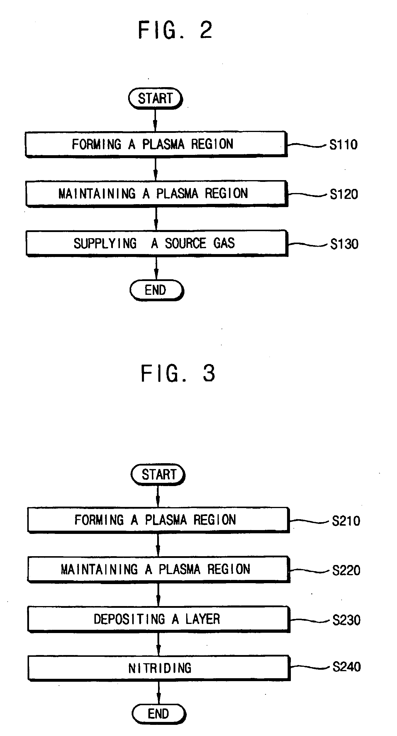
Examples
experimental example
[0141]
TABLE 3Maintenance / Formation ofDeposition ofPlasma DamageDepositionPlasma RegionPlasma RegionNitridationVoltage (Vpdm)DistributionTiCl4 Flow Rate—12sccm—0.472 V7%He Flow Rate—800sccm800sccmAr Flow Rate1,600sccm1,200sccm1,200sccmH2 Flow Rate—4,000sccm2,000sccmNH3 Flow Rate——1,500sccmRF Power350W350W600W
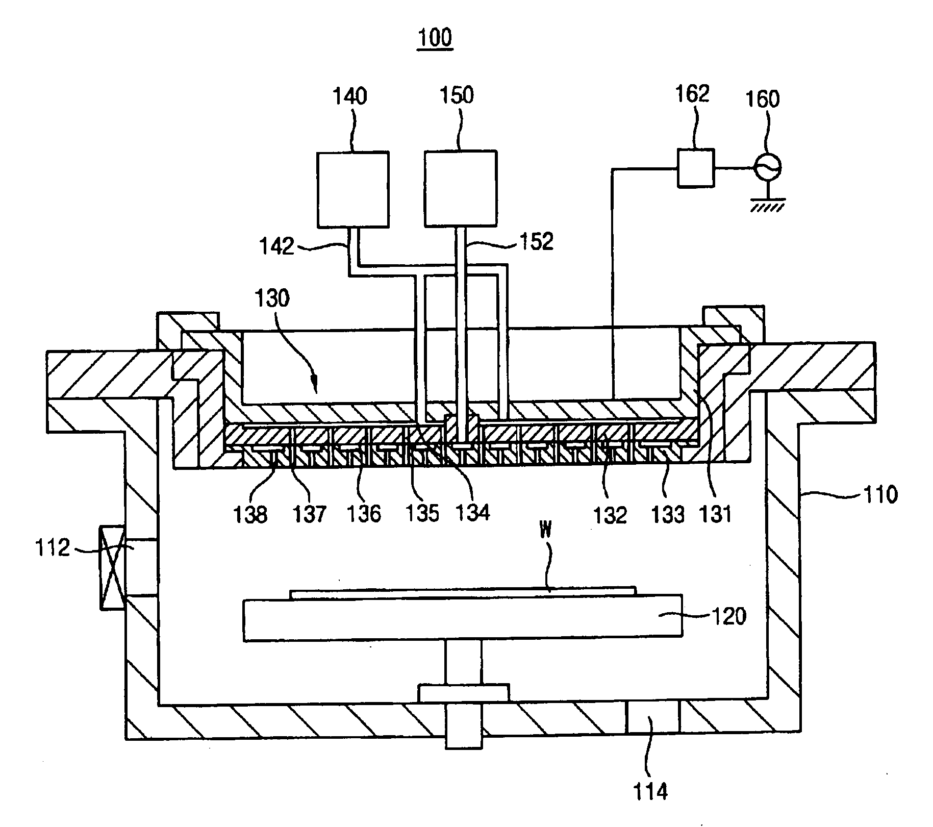
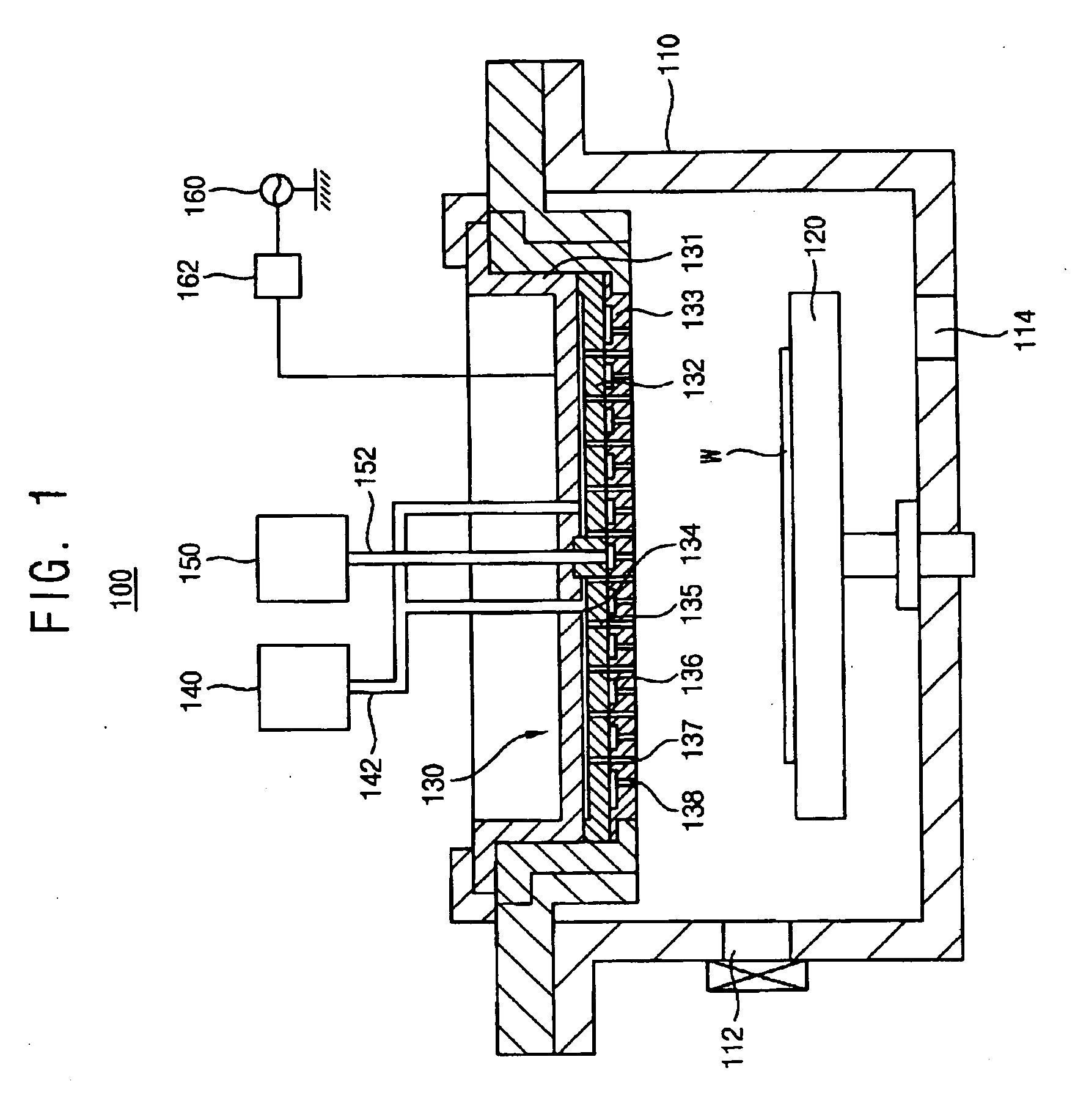
[0142] Table 3 shows results of an experimental example. In the experimental example, a plasma region was formed by supplying only argon gas to a chamber to which a high-frequency power of about 350 W was applied and maintaining the plasma region by simultaneously supplying both argon gas and helium gas, a titanium layer was formed on a wafer by supplying titanium tetrachloride (TiCl4) gas and hydrogen (H2) gas to the chamber. When the titanium layer was formed on the wafer, the titanium layer was nitrided by applying a high-frequency power of about 600 W to the chamber and supplying ammonia (NH3) gas. A measured result of plasma damage on the wafer in accordance with the experim...
PUM
| Property | Measurement | Unit |
|---|---|---|
| ionization energy | aaaaa | aaaaa |
| ionization energy | aaaaa | aaaaa |
| flow rate | aaaaa | aaaaa |
Abstract
Description
Claims
Application Information