Epoxy resin composition for encapsulating semiconductor chip and semiconductor device
Inactive Publication Date: 2007-02-22
SUMITOMO BAKELITE CO LTD
View PDF5 Cites 14 Cited by
Summary
Abstract
Description
Claims
Application Information
AI Technical Summary
This helps you quickly interpret patents by identifying the three key elements:
Problems solved by technology
Method used
Benefits of technology
Benefits of technology
[0009] The present invention has been conceived in view of the foregoing situation, and it is an object of the present invention to provide an epoxy resin composition for encapsulating a semiconductor chip having an improved flowability, an improved mold-releaseability, an improved sequential moldability and the like, and additionally having improved characteristics of a cured product thereof, such as an improved resistance to reflow soldering heat and the like, and a semiconductor device that is formed by encapsulating a semiconductor chip with the epoxy resin composition.
[0042] According to the present invention, an epoxy resin composition for encapsulating a semiconductor chip having an improved flowability,an improved mold-releaseability, an improved sequential moldability and the like, and also additionally having improved characteristics of a cured product thereof, such as an improved resistance to reflow soldering heat, a reduced water absorption and the like, is provided, as well as providing a semiconductor device that is formed by encapsulating a semiconductor chip with the epoxy resin composition.
Problems solved by technology
Based on such situation, it is the current status that requirements for epoxy resin compositions for encapsulating semiconductor chips growingly become more severe.
In particular, as a level of a reduction in thickness of a semiconductor device is increased, stress may be generated due to an incomplete mold-releasing of a cured product of the epoxy resin composition from a metal mold.
Such stress may cause a crack that are generated in the body of the semiconductor chip included in the semiconductor device and / or a reduced adhesiveness at the interface between the cured resin and the semiconductor chip.
Further, in a situation that an environmental load is a critical issue, the type of solder is switched from lead-containing solder to lead-free solder.
As such, the resistance to reflow soldering heat of a molded product, become more serious problem than in the conventional technology.
Method used
Image
Click on the blue label to locate the original text in one second.
Reading with bidirectional positioning of images and text.
Examples
examples
[0169] The present invention will be further specifically described in reference to examples as follows, though it is not intended to limit the scope of the present invention thereto.
[0170] The compositions are presented by using part by weight.
example a
Example a1
[0171] Following raw materials were employed in example a1:
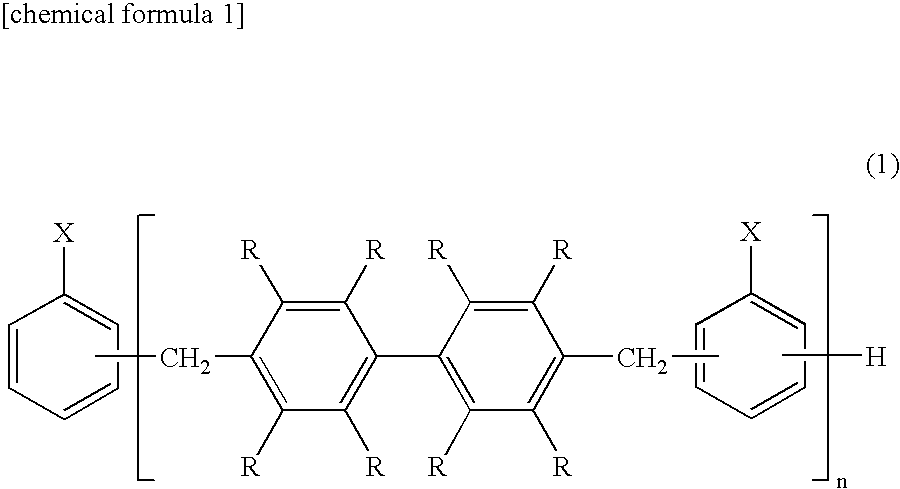
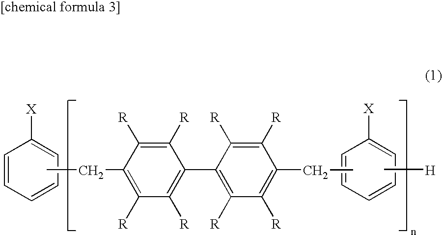
[0172] Epoxy resin represented by the following general formula (4) (phenol aralkyl type epoxy resin having biphenylene skeleton), [commercially available from Nippon Kayaku Co, Ltd., under the trade name of “NC3000P”, having softening point of 58° C. and epoxy equivalent of 273]
[0173] 7.36 parts by weight;
[0174] (n represents an average value that is a positive number within a range of from 1 to 3)
[0175] Phenolic resin of formula (5) (phenol aralkyl resin having phenylene skeleton [commercially available from Mitsui chemical Co., Ltd., under the trade name of XLC-4L, softening point of 65° C. and hydroxyl equivalent of 174]
[0176] 4.69 parts by weight
[0177] (n represents an average value that is a positive number within a range of from 1 to 3)
[0178] 1,8-diazabicyclo-(5,4,0)-undecene -7(hereinafter, referred to as “DBU”)
[0179] 0.20 parts by weight;
[0180] fused spherical silica (having mean particle diamete...
examples a2 to a23
, and Comparative Examples a1 to a9
[0197] Respective components were mixed by the ratio described in table 1, table 2 and table 3, and epoxy resin compositions were obtained in similar way as in example a1, and evaluations thereof were conducted in similar way as in example a1. Results are shown in table 1, table 2 and table 3.
[0198] Components employed in examples other than example a1 will be described as follows.
[0199] Phenolic resin of the following formula (6) (phenol aralkyl resin having biphenylene skeleton) [commercially available from Meiwa Plastic Industries Co., Ltd., under the trade name of “MEH7851SS”, softening point of 67° C., and hydroxyl equivalent of 203]
[0200] Epoxy resin of the following formula (7) (biphenyl type epoxy resin);
[0201] [commercially available from Japan epoxy resin Co., Ltd., under the trade name of YX-4000H”, melting point of 105° C., epoxy equivalent of 191]
PUM
Property
Measurement
Unit
Temperature
aaaaa
aaaaa
Temperature
aaaaa
aaaaa
Temperature
aaaaa
aaaaa
Abstract
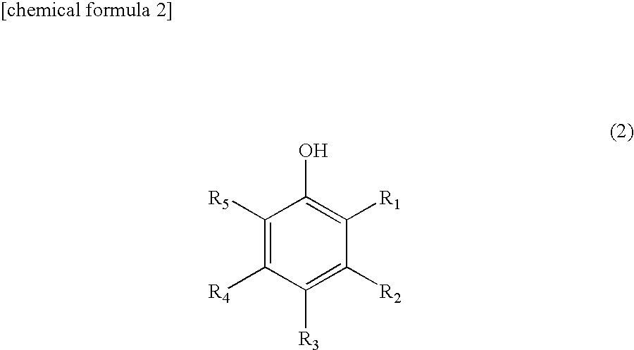
An epoxy resin composition for encapsulating a semiconductorchip having an improved flowability, an improved sequential moldability and the like, and additionally having improved characteristics of a cured product thereof, such as an improved mold-releaseability, an improved resistance to reflow soldering heat and the like, and a semiconductor device that is formed by encapsulating a semiconductorchip with the epoxy resin composition. An epoxy resin composition for encapsulating a semiconductor chip containing essential components of: (A) an epoxy resin, (B) a phenolic resin, (C) a cure accelerator, (D)an inorganic filler, (E) a mold releasing agent, (F) a silanecoupling agent and (G) a chemical compound having aromatic ring that has hydroxyl groups, each of which is bound to respective two or more adjacent carbon atoms that composes the aromatic ring. At least one of said (A) epoxy resin and said (B) phenolic resin contains resin of novolac structure, in which biphenylene skeleton is included in its main chain, and said (E) mold releasing agent includes one or more chemical compound(s) selected from a group consisting of (E1) oxidized polyethylenewax, (E2) glycerin tri-fatty acid ester and (E3) oxidized paraffin wax, and further, said (E) mold releasing agent is contained in the amount of 0.01 wt % to 1 wt % both inclusive, and said (G)chemical compound is contained in the amount of 0.01 wt % to 1 wt % both inclusive, in the total epoxy resin composition.
Description
[0001] This application is based on Japanese patent application Nos. 2005-021015 and 2005-021016, the contents of which are incorporated hereinto by reference. BACKGROUND [0002] 1. Technical Field [0003] The present invention relates to an epoxy resin composition for encapsulating a semiconductor chip and a semiconductor device employing thereof. The present invention particularly relates to an epoxy resin composition for encapsulating a semiconductor chip, which has improved characteristics such as flowability, mold-releaseability and sequential moldability, and a semiconductor device employing thereof, which has an improved the resistance to reflow soldering heat. [0004] 2. Related Art [0005] In recent years, levels of integration and surface mountability of semiconductor chips are increasing, under a situation where there are growing needs for achieving advanced functions and lighter, thinner and more compact bodies of electronic equipments. Based on such situation, it is the cur...
Claims
Application Information
Patent Timeline
Application Date:The date an application was filed.
Publication Date:The date a patent or application was officially published.
First Publication Date:The earliest publication date of a patent with the same application number.
Issue Date:Publication date of the patent grant document.
PCT Entry Date:The Entry date of PCT National Phase.
Estimated Expiry Date:The statutory expiry date of a patent right according to the Patent Law, and it is the longest term of protection that the patent right can achieve without the termination of the patent right due to other reasons(Term extension factor has been taken into account ).
Invalid Date:Actual expiry date is based on effective date or publication date of legal transaction data of invalid patent.

