

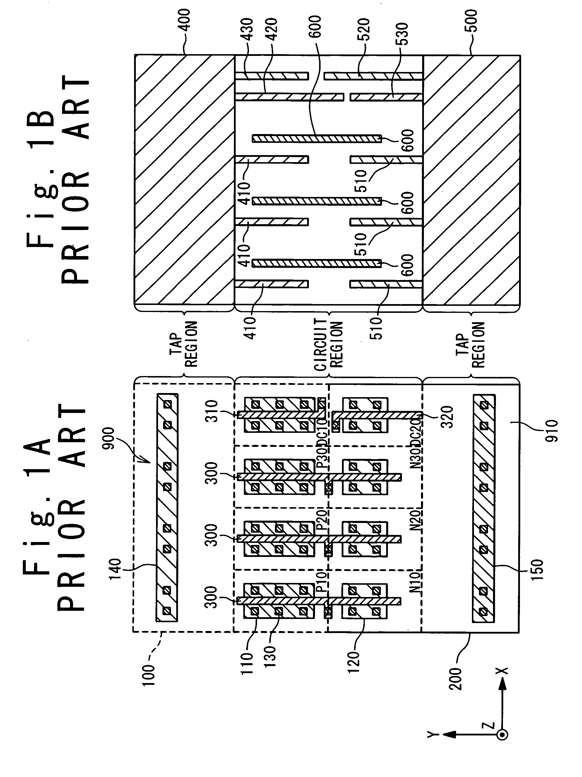
Integrated circuit incorporating decoupling capacitor under power and ground lines
a technology of integrated circuits and capacitors, applied in semiconductor devices, diodes, electrical apparatus, etc., can solve problems such as undesired increases in chip size, achieve effective suppression of power supply noise, reduce chip size, and increase width
- Summary
- Abstract
- Description
- Claims
- Application Information
AI Technical Summary
Benefits of technology
Problems solved by technology
Method used
Image

Examples
first embodiment
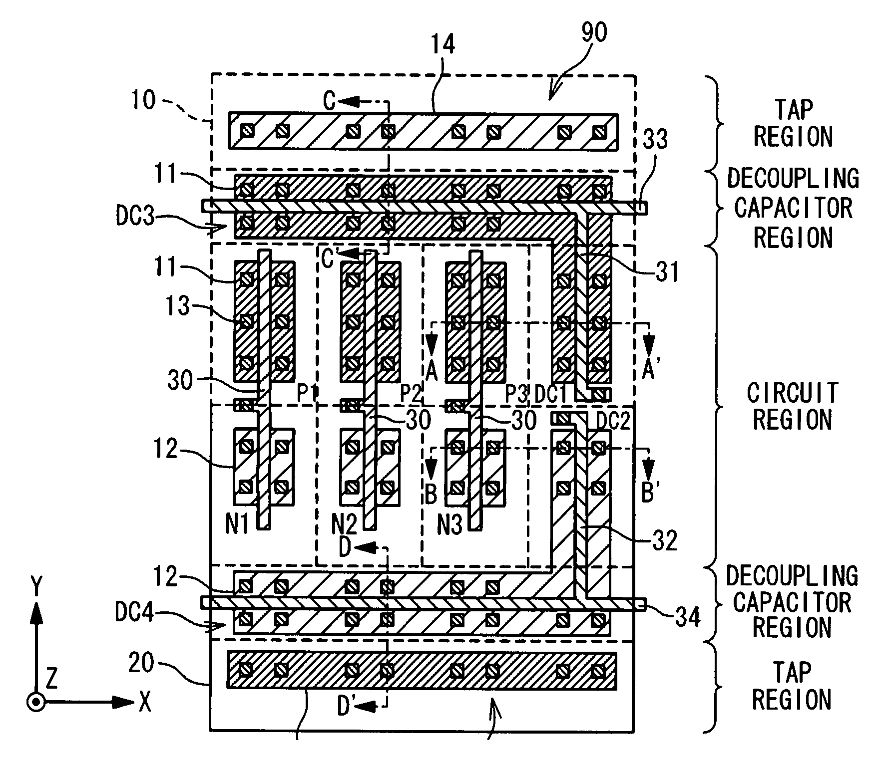
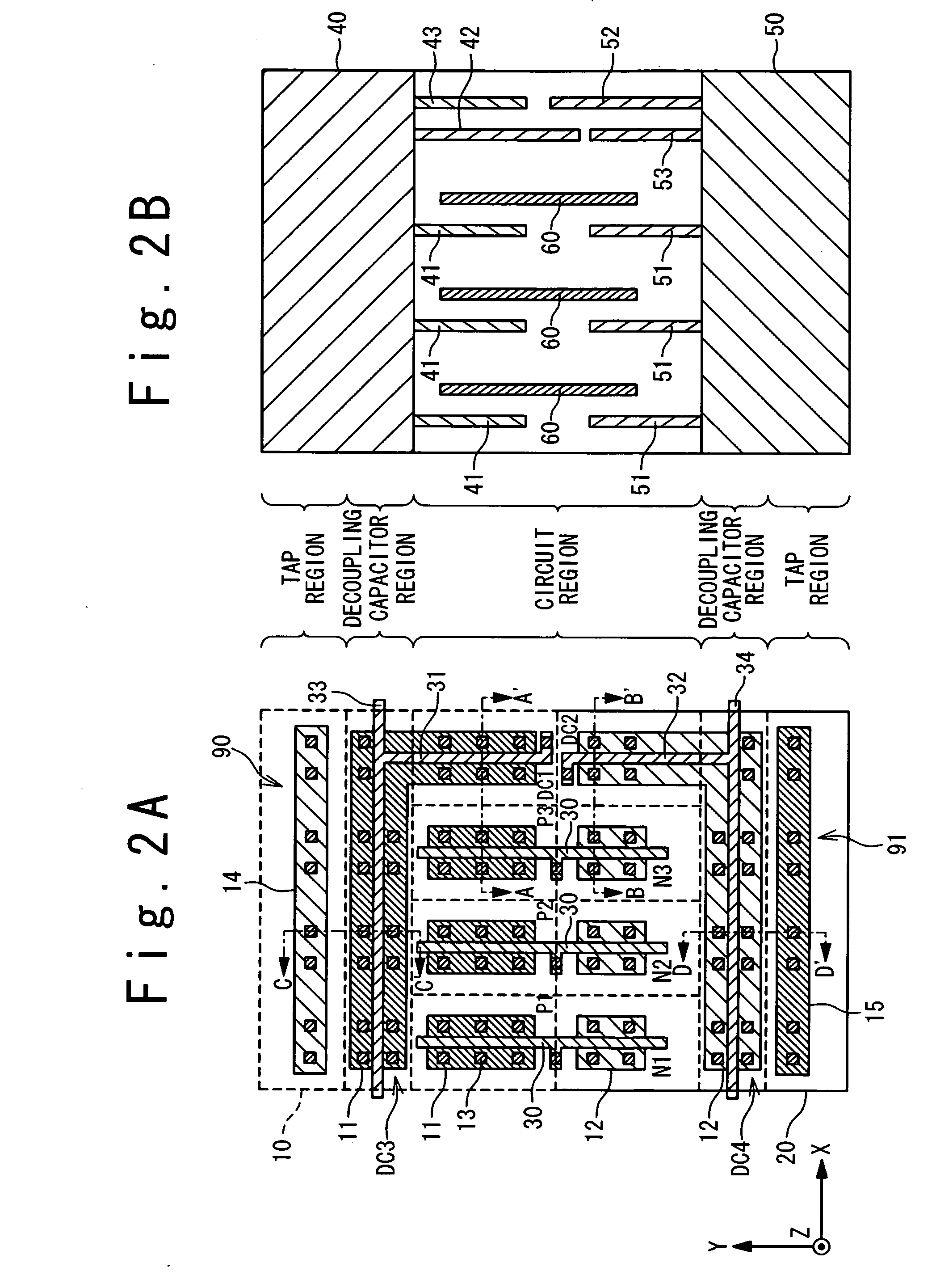
[0030]FIGS. 2A and 2B illustrate a layout of a semiconductor device in a first embodiment of the present invention. In detail, FIG. 2A illustrates layouts of a well layer, a diffusion layer, a polysilicon layer, and a contact layer, which are integrated within or on the substrate, and FIG. 2B illustrates a metal interconnection layer integrated on or over these layers.
[0031] Referring to FIG. 2A, the semiconductor device in this embodiment is composed of a circuit region, decoupling capacitor regions, and tap regions 90 and 91. An array of CMOS primitive cells are provided within the circuit region. In this embodiment, the CMOS primitive cells include CMOS inverter cells, each including a PMOS transistor and an NMOS transistor. The tap regions 90 and 91 are provided to stabilize of the electric potential of the wells of the transistors within the CMOS primitive cells.
[0032] As shown in FIG. 2B, the semiconductor device is composed of a power supply line 40 and a ground line50, whi...
second embodiment
[0048]FIGS. 8A and 8B illustrates a layout of a semiconductor device in a second embodiment of the present invention. In this embodiment, a PMOS transistor DC3′ and an NMOS transistor DC4′ are integrated under the power supply line 40 and the ground line 50, respectively, in place of the PMOS transistor DC3 and the NMOS transistor DC4 in the first embodiment.
[0049]FIG. 9 is a section view illustrating the structure on the section E-E′ indicated in FIG. 8A. The PMOS transistor DC3′ is composed of a gate electrode 33 and a pair of P-type diffusion layers 11 integrated within the N-well 10. The gate electrode 33 is electrically connected to the ground line 50 through the gate electrode 31 and the interconnection 52. One of the P-type diffusion layers 11 is used as the source of the PMOS transistor DC3′, and the other is used as the drain thereof. With respect to the PMOS transistor DC3′, only one of the P-type diffusion layers 11 is connected to the power supply line 40 through via co...
third embodiment
[0053]FIGS. 11A and 11B illustrate the layout of a semiconductor device in a third embodiment of the present invention. In the third embodiment, the N-type diffusion layer 12 within the tap region 90 is connected to a power supply line separated from the power supply line 40 connected to the CMOS primitive cells within the circuit region. Correspondingly, the P-type diffusion layer 15 within the tap region 91 is connected to a ground line separated from the ground line 50 connected the CMOS primitive cells within the circuit region.
[0054] Specifically, as shown in FIG. 11A, the layouts of the well layer, the diffusion layer, the polysilicon layer, and the contact layer are identical to those shown in FIG. 2A.
[0055] The difference is that a power supply line 80 and a ground line 90 are provided in addition to the power supply line 40 and the ground line 50, as shown in FIG. 11B. In the third embodiment, the power supply line 40 and the ground line 50 are formed to cover only the de...
PUM
 Abstract
Description
Claims
Application Information