Semiconductor device, and production method for manufacturing such semiconductor device

a semiconductor and production method technology, applied in semiconductor devices, semiconductor/solid-state device details, electrical devices, etc., can solve the problems of signal transmission delay in signal transmission path, and difficulty in completely substituting the sioch insulating layer for the silicon, so as to improve the adhesion strength

Inactive Publication Date: 2007-03-01
RENESAS ELECTRONICS CORP
View PDF5 Cites 16 Cited by
  • Summary
  • Abstract
  • Description
  • Claims
  • Application Information

AI Technical Summary

Benefits of technology

[0016] Therefore, an object of the present invention is to provide a semiconductor device having a multi-layered wiring arrangement including at least a SiOCH insulating layer covered with a thin silicon dioxide layer, in which it is possible to considerably improve an adhesion strength in an interface between the SiOCH insulating layer and the thin silicon dioxide insulating layer.
[0017] Another object of the present invention is to provide a production method for reliably and stably manufacturing such a semiconductor device.
[0020] When the insulating layer structure has a trench pattern formed therein, the metal wiring constitution comprises a metal wiring pattern buried in the trench pattern. Preferably, the metal wiring pattern is made of copper (Cu), and a barrier metal layer is formed on wall faces defining the trench pattern to thereby prevent diffusion of copper atoms from the copper wiring pattern into the insulating layer structure.
[0021] When the insulating layer structure has at least one hole formed therein, the metal wiring constitution comprises a metal via-plug buried in the hole. Preferably, the metal via-plug is made of copper (Cu), and a barrier metal layer is formed on wall faces defining the hole to thereby prevent diffusion of copper atoms from the copper via-plug into the insulating layer structure.
[0022] When the insulating layer structure has a trench pattern (108) formed therein, and at least one hole formed in a bottom of the trench pattern, and the metal wiring constitution comprises a metal wiring pattern buried in the trench pattern, and a metal via-plug buried in the hole. Preferably, the metal wiring pattern and the metal via-plug are made of copper (Cu), and a barrier metal layer is formed on wall faces defining both the trench pattern and the hole to thereby prevent diffusion of copper atoms from the copper wiring pattern and the copper via-plug into the insulating layer structure.
[0025] Preferably, the insulating layer structure further includes a barrier insulating layer on which the first SiOCH layer is formed, and the barrier insulating layer prevents diffusion of copper atoms into the first SiOCH layer when the insulating layer structure is formed on another insulating layer structure having a copper wiring constitution. The barrier insulating layer may have a single-layered structure comprising either a SiCNH layer or a SiCH layer. Also, the barrier insulating layer may have a multi-layered structure comprising a SiCNH layer and a SiCH layer. Further, the barrier insulating layer may have a multi-layered structure comprising a SiCNH layer, and a SiOCNH layer formed thereon. In addition, the barrier insulating layer may be a multi-layered structure comprising a SiCNH layer, and a SiCH layer formed thereon.

Problems solved by technology

Of course, the narrower the signal-transmission path, the larger resistance of the signal-transmission path, resulting in delay of signal transmission in the signal-transmission path.
Of course, the production of the parasitic capacitance results in delay of signal transmission in the signal-transmission paths.
In the production of the aforesaid multi-layered wiring arrangement by using the damascene process, a SiOCH insulating layer is exposed to an oxidizing atmosphere, and thus it is difficult to completely substitute the SiOCH insulating layer for the silicon dioxide insulating layer, because the SiOCH insulating layer exhibits an oxidation resistance property which is inferior to that of the silicon dioxide insulating layer.
However, an adhesion strength is relatively low in an interface between the SiOCH insulating layer and the thin silicon dioxide insulating layer, due to existence of Si—CH3 bonds on the interfacial surface of the SiOCH insulating layer, and thus both the layers are liable to be separated from each other.
Thus, both the layers are further liable to be separated from each other.
However, this plasma treatment is unsatisfactory in that it is difficult to reform and modify only a surface section of the SiOCH insulating layer.
In other words, it is very difficult to control the plasma treatment such that only the surface section of the SiOCH insulating layer is reformed and modified.
Nevertheless, the hydrogen atoms (H) are liable to be separated from the Si—H bonds in a post-treatment, because the Si—H bonds are thermally unstable.
Further, since the hydrogen atoms (H) can be easily diffused in the SiOCH insulating layer, it is very difficult to reform and modify only the surface section of the SiOCH insulating layer.
Of course, it is undesirable that the reformed and modified surface section of the SiOCH insulating layer contains moisture.

Method used


Image

  • Semiconductor device, and production method for manufacturing such semiconductor device
  • Semiconductor device, and production method for manufacturing such semiconductor device
  • Semiconductor device, and production method for manufacturing such semiconductor device

Examples


Embodiment Construction

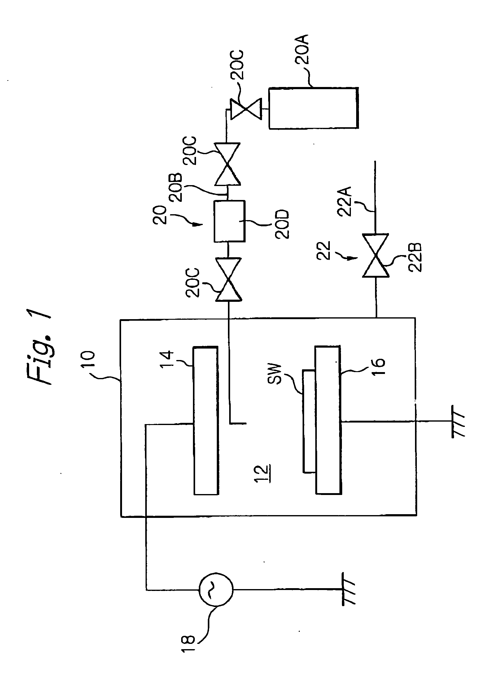
[0062] With reference to FIG. 1, a parallel-type plasma chemical vapor deposition (CVD) apparatus is schematically and conceptually illustrated. This CVD apparatus is used to manufacture semiconductor devices according to the present invention.

[0063] As shown in FIG. 1, the CVD apparatus includes a closed vessel 10 defining a processing chamber 12, a plate-like upper electrode 14 provided in the processing chamber 12, and a susceptor 16 arranged below the plate-like upper electrode 14. The CVD apparatus is provided with a radio frequency (RF) source 18 for supplying an RF power to the upper electrode 14. The susceptor 16 forms a lower electrode opposed to the upper electrode 14, and has an electric heater (not visible) incorporated therein. A semiconductor substrate to be processed, such as a silicon wafer SW, is mounted on a top surface of the susceptor or lower electrode 16, which is grounded, as shown in FIG. 1.

[0064] The CVD apparatus is also provided with a gas supply system ...


PUM


Abstract

A semiconductor device has a semiconductor substrate, and a multi-layered wiring arrangement provided thereon. The multi-layered wring arrangement includes at least one insulating layer structure having a metal wiring pattern formed therein. The insulating layer structure includes a first SiOCH layer, a second SiOCH layer formed on the first SiOCH layer, and a silicon dioxide (SiO2) layer formed on the second SiOCH layer. The second SiOCH layer features a carbon (C) density lower than that of the first SiOCH layer, a hydrogen (H) density lower than that of the first SiOCH layer, and an oxygen (O) density higher than that of the first SiOCH layer.

Description

BACKGROUND OF THE INVENTION [0001] 1. Field of the Invention [0002] The present invention relates to a semiconductor device having a multi-layered wiring arrangement produced by using a damascene process, and a production method for manufacturing such a semiconductor device. [0003] 2. Description of the Related Art [0004] In a representative process of producing a plurality of semiconductor devices, for example, a silicon wafer is prepared, and a surface of the silicon wafer is sectioned into a plurality of semiconductor chip areas by forming grid-like fine grooves (i.e. scribe lines) in the silicon wafer. Then, the silicon wafer is processed by various well-known methods such that each of the semiconductor chip areas is produced as a semiconductor device, and an insulating layer is formed as an underlayer on the semiconductor devices produced in the silicon wafer. A plurality of metal plugs are formed in an area of the insulating underlayer, which corresponds to each of the semicon...

Claims


Application Information

Patent Timeline
Patent Type & Authority Applications(United States)
IPC IPC(8): H01L23/48H01L21/4763H01L23/522H01L21/3205H01L21/768H01L23/52H01L23/532
CPCH01L23/53228H01L23/53295H01L2924/0002H01L2924/00
Inventor OHTO, KOICHIUSAMI, TATSUYAMORITA, NOBORUOHNISHI, SADAYUKIARITA, KOJIKITAO, RYOHEISASAKI, YOICHI
Owner RENESAS ELECTRONICS CORP
Why Eureka
Try Eureka