Dual port gain cell with side and top gated read transistor

Active Publication Date: 2007-03-01
GLOBALFOUNDRIES US INC
View PDF6 Cites 21 Cited by
  • Summary
  • Abstract
  • Description
  • Claims
  • Application Information

AI Technical Summary

Benefits of technology

[0004] The present invention provides a DRAM memory cell and process sequence for fabricating a dense (20 or 18 square) layout fabricated with semiconductor-on-insulator (SOI) CMOS technology. Specifically, the present invention provides a dense, high-p

Problems solved by technology

Current advances in performance of microprocessors have outpaced the performance of DRAM.
However, because of the need for larger amounts of on-chip memory, the size of the SRAM cell has made its use less attractive.
However the integration of DRAM with CMOS logic involves increased process complexity because of the competing needs of high-performance low-threshold voltage (Vt) logic devices and low-leakage DRAM array dev

Method used


Image

  • Dual port gain cell with side and top gated read transistor
  • Dual port gain cell with side and top gated read transistor
  • Dual port gain cell with side and top gated read transistor

Examples


first embodiment

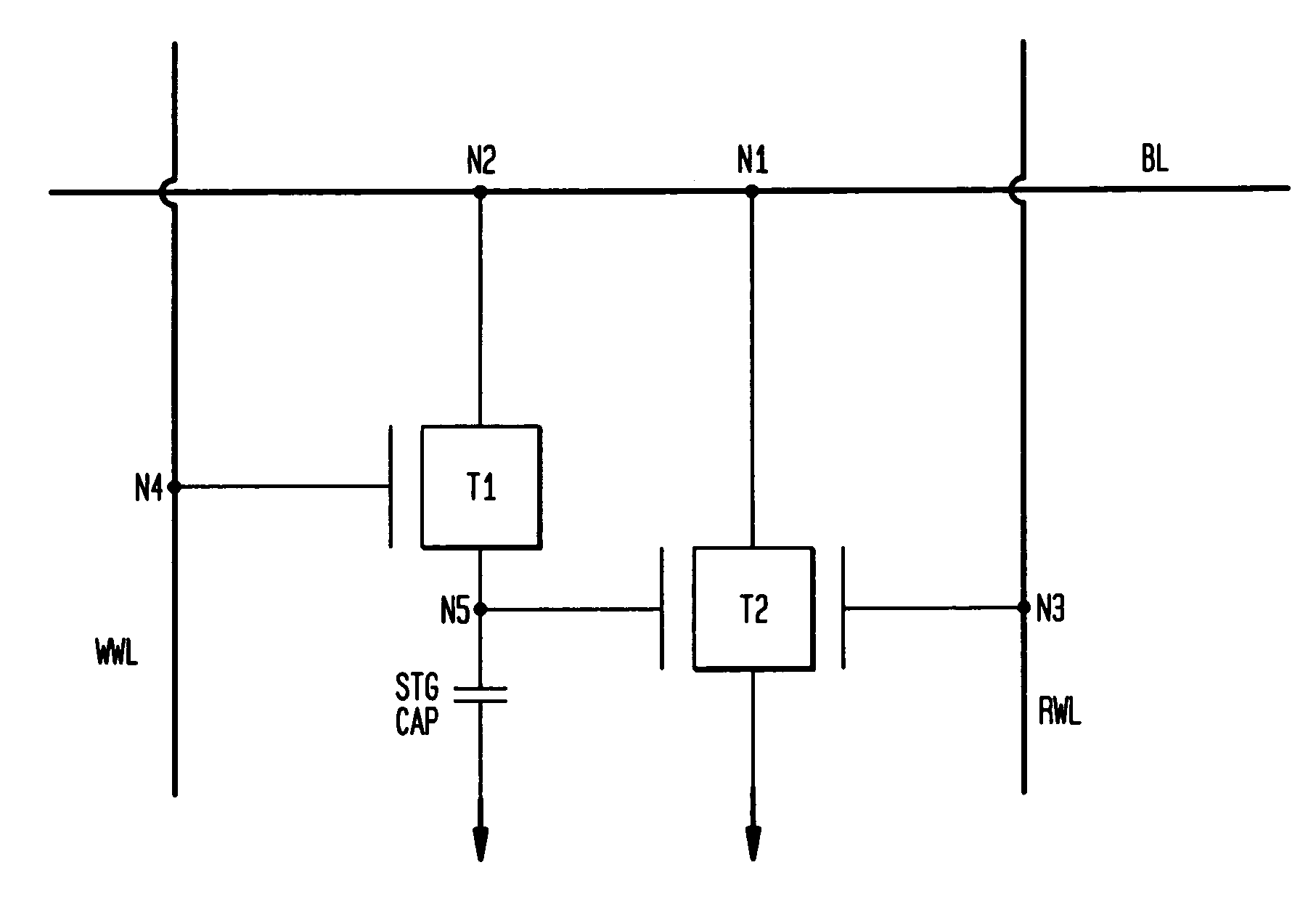
[0041] Reference is first made to FIG. 1 which shows a schematic representation of a 2T / 1C gain cell with a double gated read device in accordance with the present invention. It is emphasized that in the illustrated gain cell a transistor T2 having two gates is used. Specifically, T2 includes a side-gate that is connected to the storage node of the capacitor (STG CAP) and a top gate which is connected to the read wordline (RWL). In addition to T2, there is also shown Ti, which is the write transistor of the cell. It is observed that Ti is a conventional planar MOSFET. In the drawings, BL refers to a common bitline in which T1 and T2 are both in connection with, and WWL refers to the write wordline which is in connection with the gate of Ti.

[0042] In the cell shown in FIG. 1, a “1” or “0” is written to the storage capacitor, STG CAP, by raising the write wordline (WWL) and transferring charge between the bitline (BL) and the storage capacitor. The node of the storage capacitor serves...

second embodiment

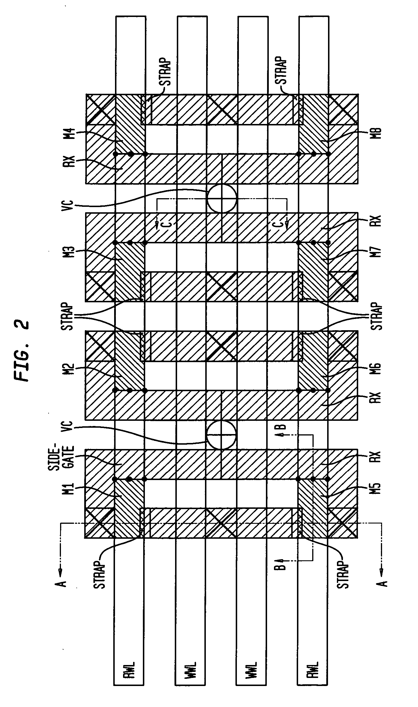
[0080]FIG. 20 is a schematic of the inventive gain cell of the present invention. Note that in the inventive gain cell shown in FIG. 20 the double-gated transistor T2 is also used. As indicated above, T2 includes two gates: a side-gate connected to the storage node of the storage trench capacitor STG CAP and a top gate connected to the RWL. This design is dual ported since a write operation, utilizing WWL and WBL, may occur simultaneously with a read, using RWL and RBL, for access. N1 . . . N5 are also shown in FIG. 20.

[0081] T1 is the write transistor and is a conventional MOSFET. A “1” or “0” is written to the storage capacitor by raising the write wordline (WWL) and transferring charge between the write bitline (WBL) and the storage capacitor. The node of the storage capacitor serves as one of the two gates of the read MOSFET T2. In this embodiment of the present invention, the node N5 gating the sidewall of T2 is integrated with the storage capacitor (STG CAP) and forms a compac...


PUM


Abstract

A DRAM memory cell and process sequence for fabricating a dense (20 or 18 square) layout is fabricated with silicon-on-insulator (SOI) CMOS technology. Specifically, the present invention provides a dense, high-performance SRAM cell replacement that is compatible with existing SOI CMOS technologies. Various gain cell layouts are known in the art. The present invention improves on the state of the art by providing a dense layout that is fabricated with SOI CMOS. In general terms, the memory cell includes a first transistor provided with a gate, a source, and a drain respectively; a second transistor having a first gate, a second gate, a source, and a drain respectively; and a capacitor having a first terminal, wherein the first terminal of said capacitor and the second gate of said second transistor comprise a single entity.

Description

FIELD OF THE INVENTION [0001] The present invention relates to a semiconductor memory cell and a method of fabricating the same. More particularly, the present invention relates to a dense, high-performance dynamic random access memory (DRAM) cell that is compatible with existing complementary metal oxide semiconductor (CMOS) technologies. BACKGROUND OF THE INVENTION [0002] Current advances in performance of microprocessors have outpaced the performance of DRAM. Because of this speed disparity, it is increasingly important to provide increasingly large amounts of cache memory on the microprocessor chip in order to meet the memory bandwidth requirements of contemporary applications. Static random access memory (SRAM) has historically been used for cache memory on processor chips because of its relative ease of process integration. However, because of the need for larger amounts of on-chip memory, the size of the SRAM cell has made its use less attractive. As SRAM memory occupies an i...

Claims


Application Information

Patent Timeline
IPC IPC(8): G11C11/24
CPCH01L27/108H01L27/1203H01L27/10867H01L27/10829H10B12/37H10B12/00H10B12/0385H10B99/00
Inventor MANDELMAN, JACKCHENG, KANGGUODIVAKARUNI, RAMACHANDRARADENS, CARLWANG, GENG
Owner GLOBALFOUNDRIES US INC
Why Eureka
Try Eureka