

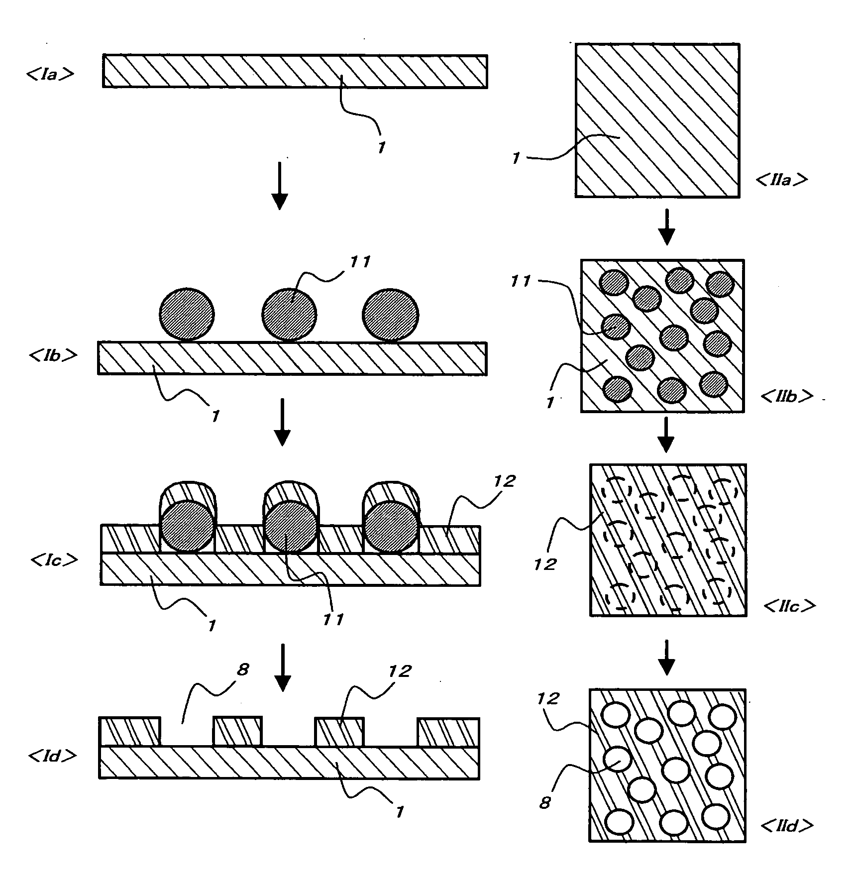
Porous thin-film-deposition substrate, electron emitting element, methods of producing them, and switching element and display element
a technology of thin film and substrate, which is applied in the manufacture of electrode systems, electric discharge tubes/lamps, and nanotechnology, etc., can solve the problems of reduced production costs, glass substrates are less resistant to impact and tend to break, and polymer films are considerably inferior to glass substrates in heat resistance and unsuitable for a process of silicon tft production
- Summary
- Abstract
- Description
- Claims
- Application Information
AI Technical Summary
Benefits of technology
Problems solved by technology
Method used
Image

Examples
example 1
[0266] [Preparation of Fine-Particle-Placed Substrate 1]
[0267] Polystyrene fine particles (Tg of bulky polystyrene is generally 100 to 110° C. and that of its particle surface is estimated approximately in a range of 70 to 80° C.) having the characteristics that the distribution of particle diameter was monodispersion, the coefficient of variation was 1.6%, the average particle diameter was 200 nm and a trimethylammonium group was provided to the surface thereof were used to prepare a dispersion liquid having a fine particle concentration of 8% by weight. This dispersion liquid was diluted with ultra-pure water into a 0.1wt % dispersion liquid, which was then desalted by dialysis. A glass substrate washed with UV / O3 was dipped in this dispersion liquid and allowed to stand at ambient temperature for 30 minutes. Then, the substrate was rinsed with boiled ultra-pure water (95° C.) for 30 seconds to carry out heat treatment, and further with ultra-pure water at ambient temperature for ...
example 2
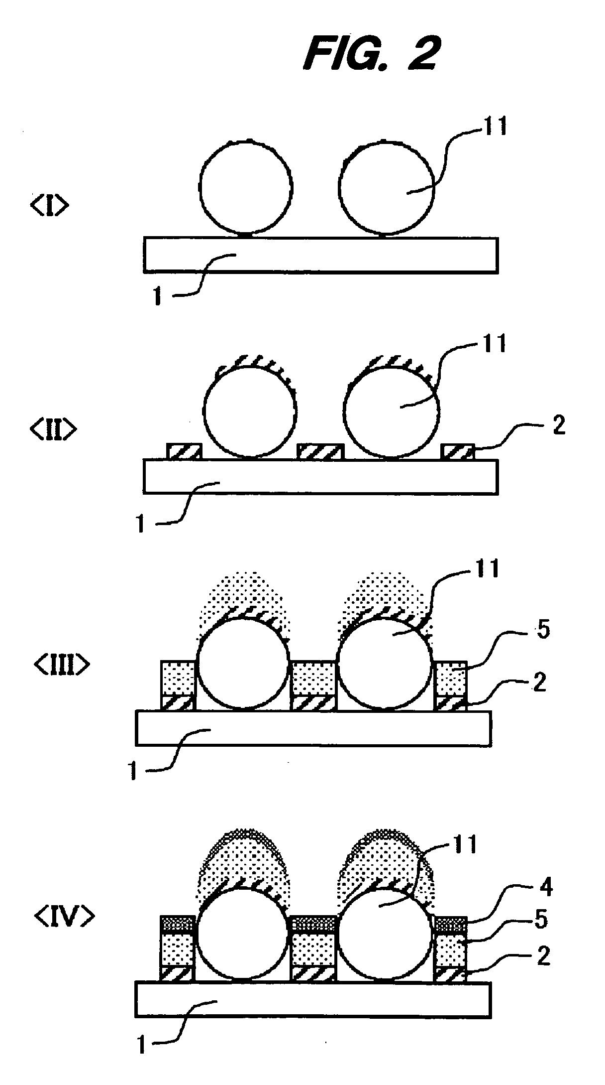
[0283] [Production of Porous Thin-Film-Deposition Substrate 2-1]
[0284] Using the fine-particle-placed substrate 1, thin films were formed in the procedures shown in FIG. 2. In specific, fine particles 11 were disposed on the substrate 1 (step I), to form a gold / chromium layer 20 nm in thickness which was to be a drain electrode 2 was formed by RF (high frequency) sputtering (step II). Next, a copper phthalocyanine layer 60 nm in thickness which was to be an organic charge transferable material layer 5 was formed by vacuum vapor deposition (organic charge transferable material layer 5: step III) and an aluminum layer 20 nm in thickness which was to be a gate electrode 4 was formed and laminated (step IV). Thereafter, an adhesive sheet was applied to the surface of the substrate and was in close contact with the substrate by making a 1.7 kg rubber roller go and back once on the adhesive sheet and then, the adhesive sheet was turned up in a direction at about 180° with the substrate to...
example 3
[0302] [Preparation of Fine-Particle-Placed Substrate]
[0303] Chromium about 1 nm in thickness was deposited as an undercoat layer 102 on a glass substrate 101 about 0.7 mm in thickness by sputtering. Tantalum about 100 nm in thickness was deposited as a cathode electrode 103 on the chromium. Nickel about 20 nm in thickness was deposited as a catalyst metal 104 on the tantalum (steps Ia and Ib in FIG. 19).
[0304] In succession, fine particles 105 which were to be a shadow mask were provided on the catalyst metal 104 by using the following method. As the fine particles, monodisperse polystyrene fine particles to the surface of which a carboxyl group was added and which had a particle diameter of 1 μm and a coefficient of variation of 3% were used. A dispersion liquid of the fine particles was adjusted to a concentration of 0.1% by weight and subjected to dialysis. The substrate was dipped in this dispersion liquid at ambient temperature for 30 minutes. Then, the substrate was rinsed w...
PUM
 Abstract
Description
Claims
Application Information